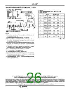
ISL6227
Pin 4 and Pin 25, the PHASE1 and PHASE2 pin
Pin 15 and Pin 16, the PG1 and PG2/REF
For dual switcher operations, these two lines are less noise
sensitive. For DDR applications, a capacitor should be
placed to the PG2/REF pin.
These traces should be short, and positioned away from other
weak signal traces. The phase node has a very high dv/dt with
a voltage swing from the input voltage to ground. No trace
should be in parallel with these traces. These traces are also
the return path for UGATE1 and UGATE2. Connect these pins
to the respective converter’s upper MOSFET source.
Pin 13, the DDR
This pin should connect to VCC in DDR applications, and to
signal ground in dual switcher applications.
Pin 5 and Pin 24, the UGATE1 and UGATE2
Pin 14, the VIN
This pin connects to battery voltage, and is less noise sensitive.
These pins have a square shape waveform with high dv/dt. It
provides the gate drive current to charge and discharge the
top MOSFET with high di/dt. This trace should wide, short,
and away from other traces similar to the LGATEx.
Copper Size for the Phase Node
Big coppers on both sides of the Phase node introduce
parasitic capacitance. The capacitance of PHASE should be
kept very low to minimize ringing. If ringing is excessive, it
could easily affect current sample information. It would be
best to limit the size of the PHASE node copper in strict
accordance with the current and thermal management of the
application.
Pin 6 and Pin 23, the BOOT1 and BOOT2
These pins di/dt are as high as that of the UGATEx;
therefore, the traces should be as short as possible.
Pin 7 and Pin 22, the ISEN1 and ISEN2
The ISEN trace should be a separate trace, and
independently go to the drain terminal of the lower MOSFET.
The current sense resistor should be close to ISEN pin.
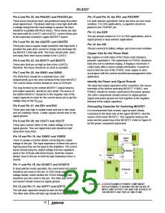
Identify the Power and Signal Ground
The input and output capacitors of the converters, the source
terminals of the bottom switching MOSFET PGND1, and
PGND2, should be closely connected to the power ground.
The other components should connect to signal ground.
Signal and power ground are tied together at the negative
terminal of the output capacitors.
The loop formed by the bottom MOSFET, output inductor,
and output capacitor, should be very small. The source of
the bottom MOSFET should tie to the negative side of the
output capacitor in order for the current sense pin to get the
voltage drop on the R
.
DSON
Pin 8 and Pin 21, the EN1 and EN2
These pins stay high in enable mode and low in idle mode
and are relatively robust. Enable signals should refer to the
signal ground.
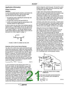
Decoupling Capacitor for Switching MOSFET
It is recommended that ceramic caps be used closely
connected to the drain side of the upper MOSFET, and the
source of the lower MOSFET. This capacitor reduces the
noise and the power loss of the MOSFET. Refer to Figure 43
for the power component placement.
Pin 9 and Pin 20, the VOUT1 and VOUT2
These pins connect either to the output voltage or to the
signal ground. They are signal lines and should be kept
away from noisy lines.
VIN
-
+
Pin 10 and Pin 19, the VSEN1 and VSEN2
There is usually a resistor divider connecting the output
voltage to this pin. The input impedance of these two pins is
high because they are the input to the amplifiers. The correct
layout should bring the output voltage from the regulation
point to the SEN pin with kelvin traces. Build the resistor
divider close to the pin so that the high impedance trace is
shorter.
-
V
o
+
Pin 11 and Pin 18, the OCSET1 and OCSET2
In dual switcher mode operation, the overcurrent set resistor
should be put close to this pin. In DDR mode operation, the
voltage divider, which divides the VDQQ voltage in half,
should be put very close to this pin. The other side of the OC
set resistor should connect to signal ground.
Lo
Lo
FIGURE 43. A GOOD EXAMPLE POWER COMPONENT
REPLACEMENT. IT SHOWS THE NEGATIVE OF
INPUT AND OUTPUT CAP AND THE SOURCE OF
THE MOSFET ARE TIED AT ONE POINT.
Pin 12 and Pin 17, the SOFT1 and SOFT2
The soft-start capacitors should be laid out close to this pin.
The other side of the soft-start cap should tie to signal ground.
25

 INTERSIL [ Intersil ]