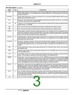
HSP50110
The Loop Filter Accumulator uses a pseudo floating point
shown in Figure 3 (see AGC Control Register, Table 9). The
format for the limits is the same as the format of the eight
most significant bits of the Loop Filter Accumulator.
Examples of how to set the limits for a specific output signal
level are provided in the “Setting DQT Gains” Section below.
NOTE: A fixed AGC gain may be set by programming
the upper and lower limits to the same value.
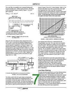
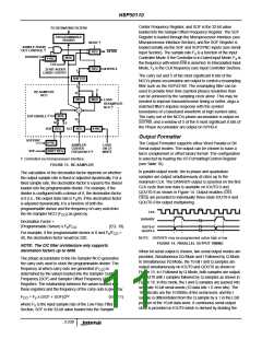
format to provide up to ~48dB of gain correction. The format
of the accumulator output is shown in Figure 3. The AGC
gain is given by:
E
Gain
= (1.0 + M) x 2
(EQ. 7)
AGC
MAPS TO AGC
UPPER AND LOWER LIMITS
256
240
224
208
192
176
160
144
128
112
96
48
42
36
30
24
18
12
6
L
2
L
2
L
2
L
2
L
2
L
2
L
2
L
2
2
1
0
-1 -2 -3 -4 -5 -6 -7 -8 -9 -10 -11 -12 -13
2
2
2
2
2
2
2
2
.
E
E
E
M
M
M
M
X
G
G
G
G
G
G
G
G
dB
MANTISSA
0.0 to 0.9375
PROGRAMMABLE
LOOP GAIN
LINEAR
EXPONENT
0 TO 7
80
64
48
32
MAPS TO µP AGC
LOOP FILTER ACCUMULATOR PARAMETER
This Value Can Be Read By The Microprocessor.
See The Microprocessor Interface Section.
16
0
0
0
16 32 48 64 80 96 112128 144160 176192 208 224 240
GAIN CONTROL WORD
(8 MSBs OF LOOP FILTER ACCUMULATOR)
FIGURE 3. BINARY FORMAT FOR LOOP FILTER
ACCUMULATOR
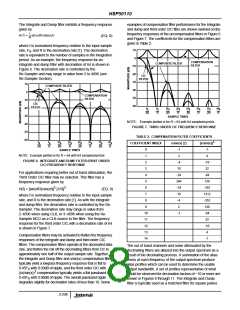
FIGURE 5. GAIN CONTROL TRANSFER FUNCTION
where M is the 4-bit mantissa value ranging from 0.0 to
The response time of the AGC is determined by the
0.9375, and E is the three bit exponent ranging from 0 to 7.
The result is a piece wise linear transfer function whose
overall response is logarithmic, as shown in Figure 5. The
exponent bits provide a coarse gain setting of 2(EEE). This
corresponds to a gain range from 0dB to 42dB (20 to 27) with
the MSB representing a 24dB gain, the next bit a 12dB gain,
and the final bit a 6dB gain. The four mantissa bits map to an
additional gain of 1.0 to 1.9375 (0 to ~6dB). Together, the
exponent and the mantissa portion of the limit set a gain
range from 0 to ~48dB.
Programmable Loop Gain. The Loop Gain is an unsigned
8-bit value whose significance relative to the AGC gain is
shown in Figure 3. The loop gain is added or subtracted from
the accumulator depending on the output of the Level
Detector. The accumulator is updated at the output sample
rate. If the accumulator exceeds the upper or lower limit, the
accumulator is loaded with that limit. The slew rate of the
AGC ranges between ~0.001dB and 0.266dB per output
sample for Loop Gains between 01(HEX) and FF (HEX)
respectively.
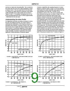
AGC
DISABLE †
AGC L.D. SENSE†
AGC THRESHOLD †
The user should exercise care when using maximum loop
gain when the (x/sin(x)) or the (x/sin(x)) compensation filter is
3
AGC LOOP FILTER
enabled. At high decimation rates, the delay through the
compensation filter may be large enough to induce
oscillations in the AGC loop. The Basic Architectural
Configurations Section contains the necessary detailed block
diagrams to determine the loop delay for different matched
filter configurations.
LEVEL
DETECTOR
REG
LIMIT
REG
+
LOWER
GAIN
LIMIT †
UPPER
GAIN
LIMIT †
Q DATA
I DATA
PROGRAMMABLE
LOOP GAIN †
Low Pass Filtering
The gain corrected signal feeds a Low Pass Filtering Section
comprised of a Cascaded Integrator Comb (CIC) and
compensation filter. The filtering section extracts the channel
of interest while providing decimation to match the output
sample rate to the channel bandwidth. A variety of filtering
configurations are possible which include integrate and
dump, integrate and dump with x/sin(x) compensation, third
order CIC, and third order CIC with ((x)/sin(x))3
† Indicates data downloaded via microprocessor interface.
FIGURE 4. AGC BLOCK DIAGRAM
The limiter restricts the AGC gain range by keeping the
accumulator output between the programmed limits. If the
accumulator exceeds the upper or lower limit, then the
accumulator is held to that limit. The limits are programmed
via eight bit words which express the values of the upper and
lower limits as eight bit pseudo floating point numbers as
compensation. If none of these filtering options are desired,
the entire filtering section may be bypassed.
3-235

 INTERSIL [ Intersil ]