HSP50110
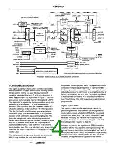
The quadrature outputs of the NCO are generated by driving
where PO is the 8-bit two’s complement value loaded into the
Phase Offset Register (see Phase Offset Register in Table 6).
a sine/cosine lookup table with the output of a phase
accumulator as shown in Figure 2. Each time the phase
accumulator is clocked, its sum is incremented by the sum of
the contents of the Carrier Frequency (CF) Register and the
Carrier Offset Frequency (COF) Register. As the
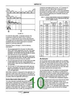
As an example, a value of 32, (20
Phase Offset Register would produce a phase offset of 45 .
), loaded into the
HEX
o
An alternative method for controlling the NCO Phase uses
o
the PH0-1 inputs to shift the phase of NCO’s output by 0 ,
32
accumulator sum transitions from 0 to 2 , the SIN/COS
o
o
o
90 , 180 , or 270 . The PH0-1 inputs are mapped to phase
shifts as shown in Table 1. The phase may be updated every
clock supporting the π/2 phase shifts required for modulation
or despreading of CDMA signals.
ROM produces quadrature outputs whose phase advances
o
o
from 0 to 360 . The sum of the CF and COF Registers
represent a phase increment which determines the
frequency of the quadrature outputs. Large phase
-36
increments take fewer clocks to transition through the sine
wave cycle which results in a higher frequency NCO output.
The output of the complex multiplier is scaled by 2 . See
“Setting DQT Gains” below.
TABLE 1. PH0-1 INPUT PHASE MAPPING
The NCO frequency is set by loading the CF and COF
Registers. The contents of these registers set the NCO
frequency as given by the following,
PH1-0
00
PHASE SHIFT
o
0
F
= F x (CF + COF)/232,
(EQ. 5)
C
S
o
01
90
where f is the sample rate set by the Input Controller, CF is
S
o
10
270
the 32-bit two’s complement value loaded into the Carrier
Frequency Register, and COF is the 32-bit two’s
complement value loaded into the Carrier Offset Frequency
Register. This can be rewritten to have the programmed CF
and COF value on the left:
o
11
180
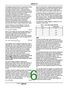
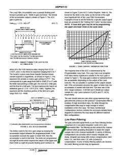
AGC
The level of the Mixer output is gain adjusted by an AGC
closed around the Low Pass Filtering. The AGC provides the
coarse gain correction necessary to help maintain the output
of the HSP50110 at a signal level which maintains an
acceptable dynamic range. The AGC consists of a Level
Detector which generates an error signal, a Loop Gain
multiplier which amplifies the error, and a Loop Filter which
integrates the error to produce gain correction (see
Figure 4).
32
(EQ. 5A)
(CF + COF) = INT[(F /F )2
]
HEX
C
S
As an example, if the CF Register is loaded with a value of
3000 0000 (Hex), the COF Register is loaded with a value of
1000 0000 (Hex), and the input sample rate is 40 MSPS, an
the NCO would produce quadrature terms with a frequency
of 10MHz. When the sum of CF and COF is a negative
value, the cos/sin vector generated by the NCO rotates
clockwise which downconverts the upper sideband; when
the sum is positive, the cos/sin vector rotates
counterclockwise which upconverts the lower sideband.
Note: the input sample rate F is determined by the rate
at which ENI is asserted low (see Input Controller
Section). If ENI is tied low, the input sample rate is equal
to the CLK rate.
The Level Detector generates an error signal by comparing the
magnitude of the DQT output against a user programmable
threshold (see AGC Control Register in Table 9). In the normal
mode of operation, the Level Detector outputs a -1 for
magnitudes above the threshold and +1 for those below the
threshold. The ±1 outputs are then multiplied by a
programmable loop gain to generate the error signal integrated
by the Loop Filter. The Level Detector uses the magnitude
estimation algorithm described in the Input Level Detector
Section. The sense of the Level Detector Output may be
changed via the Chip Configuration Register, bit 0 (see Table
12).
S
The Carrier Frequency Register is loaded via the
Microprocessor Interface and the Carrier Offset Frequency is
loaded serially using the COF and COFSYNC inputs. The
procedure for loading these registers is discussed in the
Microprocessor Interface Section and the Serial Input
Section.
The Loop Filter consists of a multiplier, an accumulator and a
programmable limiter. The multiplier computes the product of
the output of the Level Detector and the Programmable Loop
Gain. The accumulator integrates this product to produce the
AGC gain, and the limiter keeps the gain between preset
limits (see AGC Control Register, Table 9). The output of the
AGC Loop Filter Accumulator can be read via the
The phase of the NCO’s quadrature outputs can be adjusted
by adding an offset value to the output of the phase
accumulator as shown in Figure 2. The offset value can be
loaded into the Phase Offset (PO) Register or input via the
PH0-1 inputs. If the PO Register is used, the phase can be
o
adjusted from -π to π with a resolution of ~1.4 . The phase
Microprocessor Interface to estimate signal strength (see
Microprocessor Interface Section).
offset is given by the following equation,
φ = π x (PO/128),
(EQ. 6)
3-234

 INTERSIL [ Intersil ]