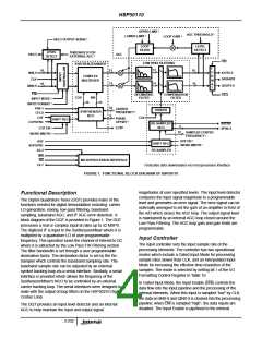
HSP50110
Pin Description (Continued)
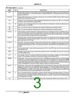
NAME
TYPE
DESCRIPTION
SOF
I
Sampler Offset Frequency. This serial input is used to load the Sampler Offset Frequency into the Re-Sampler NCO
(see Serial Interface Section). The new offset frequency is shifted in MSB first by CLK starting with the clock cycle after
assertion of SOFSYNC.
SOFSYNC
A2-0
I
I
Sampler Offset Frequency Sync. This signal is asserted one CLK cycle before the MSB of Sampler Offset Frequency
data word (see Serial Interface Section).
Address Bus. These inputs specify a target register within the Microprocessor Interface (see Table 5). A2 is the MSB.
This input is setup and held to the rising edge of WR.
C7-0
I/0
Control Bus. This is the bidirectional data bus for reads and writes to the Microprocessor Interface (see Microprocessor
Interface Section). C7 is the MSB.
WR
RD
I
I
Write. This is the write strobe for the Microprocessor Interface (see Microprocessor Interface Section).
Read. This is the read enable for the Microprocessor Interface (see Microprocessor Interface Section).
IOUT9-0
O
In-Phase Output. The data on these pins is output synchronous to CLK. New data on IOUT9-0 is indicated by the as-
sertion of the DATARDY pin. Data may be output parallel or serial mode (see Output Formatter Section). In the parallel
mode, IOUT9 is the MSB. When the serial mode is used, IOUT0 is data, and IOUT9 is the serial clock. Other pins not
used in serial mode may be set high or low via the control interface.
QOUT9-0
O
O
Quadrature Output. The data on these pins is output synchronous to CLK. New data on the QOUT(9-0) pins is indicated
by the DATARDY pin. Data may be output parallel or serial mode. In the parallel mode, IOUT9 is the MSB. When the
serial mode is used, QOUT0 is data.
DATARDY
Data Ready. This output is asserted on the first clock cycle that new data is available on the IOUT and QOUT data
busses (see Output Formatter Section). This pin may be active ‘high’ or ‘low’ depending on the configuration of the I/O
Formatting/Control Register (see Table 10). In serial mode, DATARDY is asserted one IQ clock before for first bit of se-
rial data.
OEI
OEQ
I
I
In-Phase Output Enable. This pin is the three-state control for IOUT9-0. When OEI is ‘high’, the IOUT bus is held in the
high impedance state.
Quadrature Output Enable. This pin is the three-state control for QOUT9-0. When OEQ is ‘high’, the QOUT bus is held
in the high impedance state.
LOTP
SSTRB
0
0
Local Oscillator Test Point. This output is the MSB of the Synthesizer NCO phase accumulator (see Synthesizer/Mixer
Section). This is provided as a test point for monitoring the frequency of the Synthesizer NCO.
Sample Strobe. This is the bit rate strobe for the bit rate NCO. SSTRB has two modes of operation: continuous update
and sampled. In continuous update mode, this is the carry output of the Re-Sampler NCO. In sampled mode, SSTRB
is active synchronous to the DATARDY signal for parallel output mode. The sampled mode is provided to signal the
nearest output sample aligned with or following the symbol boundary. This signal can be used with SPH(4-0) below to
control a resampling filter to time shift its impulse response to align with the symbol boundaries.
SPH4-0
0
Sample Phase. These are five of the most significant 8 bits of the Re-Sampler NCO phase accumulator. Which five bits
of the eight is selected via the Chip Configuration Register (see Table 12). These pins update continuously when the
SSTRB output is in the continuous update mode. When the SSTRB pin is in the sampled mode, SPH4-0 update only
when the SSTRB pin is asserted. In the sampled mode, these pins indicate how far the bit phase has advanced past
the symbol boundary when the output sample updates. SPH4 is the MSB.
HI/LO
CLK
0
I
HI/LO. The output of the Input Level Detector is provided on this pin (see Input Level Detector Section). The sense of
the HI/LO pin is set via the Chip Configuration Register (see Table 12). This signal can be externally averaged and used
to control the gain of an amplifier to close an AGC loop around the A/D converter. This type of AGC sets the level based
on the median value on the input.
Clock. All I/O’s with the exception of the output enables and the microprocessor interface are synchronous to clock.
3-231

 INTERSIL [ Intersil ]