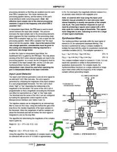
HSP50110
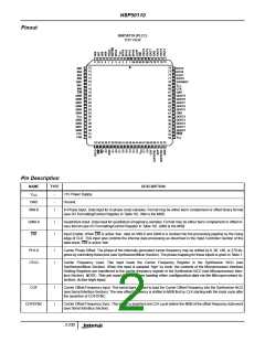
Pinout
HSP50110 (PLCC)
TOP VIEW
11 10 9
8 7 6 5 4 3 2 1 84 83 82 81 80 79 78 77 76 75
12
13
14
15
16
17
18
19
20
21
22
23
24
25
26
27
28
29
30
31
32
74
73
72
71
70
69
68
67
66
65
64
63
62
61
60
59
58
57
56
55
54
IIN5
IIN4
IIN3
IIN2
GND
IIN1
IOUT3
IOUT2
IOUT1
IOUT0
DATARDY
V
CC
IIN0
ENI
CLK
GND
QIN9
QIN8
QIN7
QIN6
QIN5
QIN4
QOUT9
QOUT8
QOUT7
QOUT6
QOUT5
GND
QOUT4
QOUT3
QOUT2
QOUT1
QOUT0
OEQ
V
CC
QIN3
QIN2
QIN1
QIN0
PH1
PH0
V
CC
33 34 35 36 37 38 39 40 41 42 43 44 45 46 47 48 49 50 51 52 53
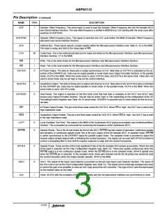
Pin Description
NAME
TYPE
DESCRIPTION
V
-
-
I
+5V Power Supply.
Ground.
CC
GND
IIN9-0
In-Phase Input. Data input for in-phase (real) samples. Format may be either two’s complement or offset binary format
(see I/O Formatting/Control Register in Table 10). IIN9 is the MSB.
QIN9-0
ENI
I
I
Quadrature Input. Data input for quadrature (imaginary) samples. Format may be either two’s complement or offset bi-
nary format (see I/O Formatting/Control Register in Table 10). QIN9 is the MSB.
Input Enable. When ENI is active ‘low’, data on IIN9-0 and QIN9-0 is clocked into the processing pipeline by the rising
edge of CLK. This input also controls the internal data processing as described in the Input Controller Section of the
data sheet. ENI is active ‘low’.
PH1-0
CFLD
I
I
Carrier Phase Offset. The phase of the internally generated carrier frequency may be shifted by 0, 90, 180, or 270 de-
grees by controlling these pins (see Synthesizer/Mixer Section). The phase mapping for these inputs is given in Table 1.
Carrier Frequency Load. This input loads the Carrier Frequency Register in the Synthesizer NCO (see
Synthesizer/Mixer Section). When this input is sampled ‘high’ by clock, the contents of the Microprocessor Interface
Holding Registers are transferred to the carrier frequency register in the Synthesizer NCO (see Microprocessor Inter-
face Section). NOTE: This pin must be ‘low’ when loading other configuration data via the Microprocessor In-
terface. Active high Input.
COF
I
I
Carrier Offset Frequency Input. This serial input is used to load the Carrier Offset Frequency into the Synthesizer NCO
(see Serial Interface Section). The new offset frequency is shifted in MSB first by CLK starting with the clock cycle after
the assertion of COFSYNC.
COFSYNC
Carrier Offset Frequency Sync. This signal is asserted one CLK cycle before the MSB of the offset frequency data word
(see Serial Interface Section).
3-230

 INTERSIL [ Intersil ]