BBT3821
IEEE PMA/PMD REGISTERS (1.0 TO 1.15/1.000F’H)
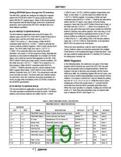
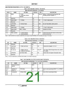
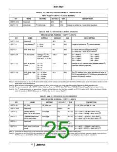
Table 5. IEEE PMA/PMD CONTROL 1 REGISTER
MDIO REGISTER ADDRESS = 1.0 (1.0000’h)
BIT(S)
NAME
SETTING
DEFAULT
0’b
R/W
DESCRIPTION
1.0.15
3.0.15
4.0.15
Reset
1 = reset
R/W SC Writing 1 to this bit will reset the whole chip,
(1)
0 = reset done, normal
operation
including the MDIO registers.
1.0.14
1.0.13
1.0.12
1.0.11
1.0.10:7
1.0.6
Reserved
0’b
1’b
0’b
0’b
0’h
1’b
0’h
0’b
0’b
Speed Select
Reserved
1 = 10Gbps
RO
1 = bits 5:2 select speed
LOPOWER
Reserved
0 = Normal Power
R/W
No Low Power Mode, writes ignored
Speed Select
Speed Select
Reserved
1 = 10Gbps
RO
RO
1 = bits 5:2 select speed
Operates at 10Gbps
1.0.5:2
1.0.1
0000 = 10Gbps
1.0.0
PMA Loopback
1 = Enable loopback
0 = Normal operation
R/W
Enable serial loop back mode on all four lanes,
XAUI in to XAUI out.
Note (1): After this RESET bit is written, the BBT3821 will not begin counting PREAMBLE bits immediately. See Figure 17 for details.
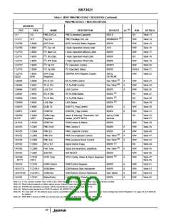
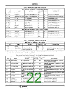
Table 6. IEEE PMA/PMD STATUS 1 REGISTER
MDIO REGISTER ADDRESS = 1.1 (1.0001’h)
BIT
1.1.15:8
1.1.7
NAME
Reserved
SETTING
DEFAULT
00’h
R/W
DESCRIPTION
Local Fault
Reserved
Rx Link Up
1 = PMA Local Fault
0’b
0’h
1’b
RO
Derived from Register 1.8.11:10
1.1.6:3
1.1.2
(1)
(1)
1 = PMA Rx Link Up
0 = PMA/D Rx Link Down
RO LL
RO
‘Up’ means CX4/LX4 signal level is OK, and the
PLL locked
1.1.1
1.1.0
LoPwrAble
Reserved
Low Power Ability
0’b
0’b
Device does not support a low power mode
Note (1): This bit is latched low on a detected Fault condition. It is set high on being read.
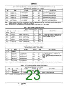
Table 7. IEEE PMA/PMD, PCS, PHY XS, SPEED ABILITY REGISTER
MDIO REGISTER ADDRESSES = 1.4, 3.4 & 4.4 ([1,3,4].0004’h)
BIT
NAME
SETTING
DEFAULT
000’h
R/W
DESCRIPTION
1.4.15:3
3.4.15:2
4.4.15:1
Reservedforfuture
speeds
1.4.2:1
3.4.1
10PASS-T2/
2BASE-TL
EFM Ability
10Gbps Ablility
00’b
1’b
RO
RO
Device cannot operate @ 2BASE-TL or 10PASS-
T2
1.4.0
3.4.0
4.4.0
10GbpsAble
Device Able to operate @ 10Gbps
21

 INTERSIL [ Intersil ]