1-Gbit P30 Family
10.0
Read Operations
The device supports two read modes: asynchronous page mode and synchronous burst mode.
Asynchronous page mode is the default read mode after device power-up or a reset. The Read
Configuration Register must be configured to enable synchronous burst reads of the flash memory
array (see Section 10.3, “Read Configuration Register” on page 54).
The device can be in any of four read states: Read Array, Read Identifier, Read Status or Read
Query. Upon power-up, or after a reset, the device defaults to Read Array. To change the read state,
the appropriate read command must be written to the device (see Section 9.2, “Device Commands”
on page 50). See Section 14.0, “Special Read States” on page 75 for details regarding Read Status,
Read ID, and CFI Query modes.
The following sections describe read-mode operations in detail.
10.1
Asynchronous Page-Mode Read
Following a device power-up or reset, asynchronous page mode is the default read mode and the
device is set to Read Array. However, to perform array reads after any other device operation (e.g.
write operation), the Read Array command must be issued in order to read from the flash memory
array.
Note:
Asynchronous page-mode reads can only be performed when Read Configuration Register bit
RCR[15] is set (see Section 10.3, “Read Configuration Register” on page 54).
To perform an asynchronous page-mode read, an address is driven onto the Address bus, and CE#
and ADV# are asserted. WE# and RST# must already have been deasserted. WAIT is deasserted
during asynchronous page mode. ADV# can be driven high to latch the address, or it must be held
low throughout the read cycle. CLK is not used for asynchronous page-mode reads, and is ignored.
If only asynchronous reads are to be performed, CLK should be tied to a valid VIH level, WAIT
signal can be floated and ADV# must be tied to ground. Array data is driven onto DQ[15:0] after
an initial access time tAVQ V delay. (see Section 7.0, “AC Characteristics” on page 33).
In asynchronous page mode, four data words are “sensed” simultaneously from the flash memory
array and loaded into an internal page buffer. The buffer word corresponding to the initial address
on the Address bus is driven onto DQ[15:0] after the initial access delay. The lowest two address
bits determine which word of the 4-word page is output from the data buffer at any given time.
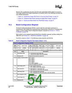
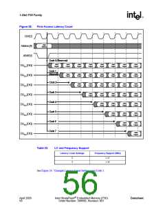
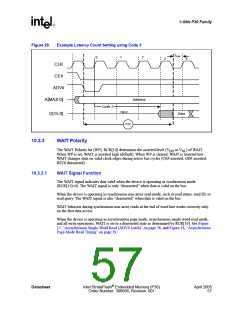
10.2
Synchronous Burst-Mode Read
To perform a synchronous burst- read, an initial address is driven onto the Address bus, and CE#
and ADV# are asserted. WE# and RST# must already have been deasserted. ADV# is asserted, and
then deasserted to latch the address. Alternately, ADV# can remain asserted throughout the burst
access, in which case the address is latched on the next valid CLK edge while ADV# is asserted.
During synchronous array and non-array read modes, the first word is output from the data buffer
on the next valid CLK edge after the initial access latency delay (see Section 10.3.2, “Latency
Count” on page 55). Subsequent data is output on valid CLK edges following a minimum delay.
Datasheet
Intel StrataFlash® Embedded Memory (P30)
Order Number: 306666, Revision: 001
April 2005
53

 INTEL [ INTEL ]