1-Gbit P30 Family
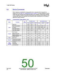
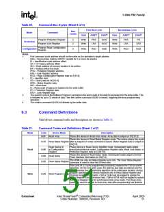
Table 20.
Command Bus Cycles (Sheet 2 of 2)
First Bus Cycle
Second Bus Cycle
Bus
Command
Mode
Cycles
Oper
Addr(1)
Data(2)
Oper
Addr(1)
Data(2)
Program Protection Register
Program Lock Register
2
2
Write
Write
PRA
LRA
0xC0
0xC0
Write
Write
PRA
LRA
PD
Protection
LRD
Program Read Configuration
Register
Configuration
2
Write
RCD
0x60
Write
RCD
0x03
Notes:
1.
First command cycle address should be the same as the operation’s target address.
DBA = Device Base Address (NOTE: needed for 2 or more die stacks)
IA = Identification code address offset.
QA = CFI Query address offset.
WA = Word address of memory location to be written.
BA = Address within the block.
PRA = Protection Register address.
LRA = Lock Register address.
RCD = Read Configuration Register data on A[15:0].
ID = Identifier data.
2.
QD = Query data on DQ[15:0].
SRD = Status Register data.
WD = Word data.
N = Word count of data to be loaded into the write buffer.
PD = Protection Register data.
LRD = Lock Register data.
3.
4.
The second cycle of the Buffered Program Command is the word count of the data to be loaded into the write buffer. This
is followed by up to 32 words of data.Then the confirm command (0xD0) is issued, triggering the array programming
operation.
The confirm command (0xD0) is followed by the buffer data.
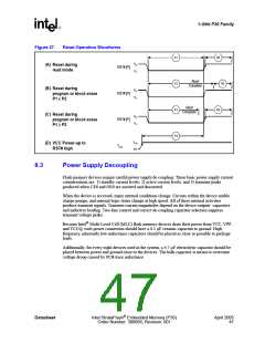
9.3
Command Definitions
Valid device command codes and descriptions are shown in Table 21.
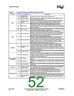
Table 21.
Command Codes and Definitions (Sheet 1 of 2)
Mode
Code
Device Mode
Description
0xFF Read Array
Places the device in Read Array mode. Array data is output on DQ[15:0].
Places the device in Read Status Register mode. The device enters this mode
0x70 Read Status Register after a program or erase command is issued. Status Register data is output on
DQ[7:0].
Read Device ID
0x90 or Configuration
Register
Places device in Read Device Identifier mode. Subsequent reads output
manufacturer/device codes, Configuration Register data, Block Lock status, or
Protection Register data on DQ[15:0].
Read
Places the device in Read Query mode. Subsequent reads output Common
Flash Interface information on DQ[7:0].
0x98 Read Query
The WSM can only set Status Register error bits. The Clear Status Register
command is used to clear the SR error bits.
0x50 Clear Status Register
First cycle of a 2-cycle programming command; prepares the CUI for a write
operation. On the next write cycle, the address and data are latched and the
WSM executes the programming algorithm at the addressed location. During
program operations, the device responds only to Read Status Register and
Program Suspend commands. CE# or OE# must be toggled to update the
Status Register in asynchronous read. CE# or ADV# must be toggled to update
the Status Register Data for synchronous Non-array reads. The Read Array
command must be issued to read array data after programming has finished.
Write
0x40 Word Program Setup
Datasheet
Intel StrataFlash® Embedded Memory (P30)
Order Number: 306666, Revision: 001
April 2005
51

 INTEL [ INTEL ]