1-Gbit P30 Family
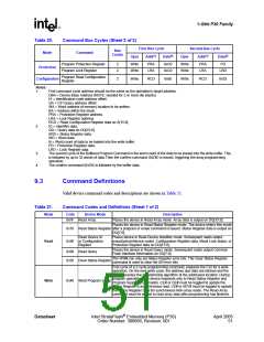
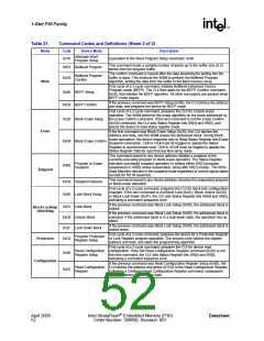
Table 21.
Command Codes and Definitions (Sheet 2 of 2)
Mode
Code
Device Mode
Description
Alternate Word
Program Setup
0x10
Equivalent to the Word Program Setup command, 0x40.
This command loads a variable number of words up to the buffer size of 32
words onto the program buffer.
0xE8 Buffered Program
The confirm command is Issued after the data streaming for writing into the
buffer is done. This instructs the WSM to perform the Buffered Program
algorithm, writing the data from the buffer to the flash memory array.
Buffered Program
Confirm
0xD0
Write
First cycle of a 2-cycle command; initiates Buffered Enhanced Factory
Program mode (BEFP). The CUI then waits for the BEFP Confirm command,
0xD0, that initiates the BEFP algorithm. All other commands are ignored when
BEFP mode begins.
0x80 BEFP Setup
If the previous command was BEFP Setup (0x80), the CUI latches the address
and data, and prepares the device for BEFP mode.
0xD0 BEFP Confirm
First cycle of a 2-cycle command; prepares the CUI for a block-erase
operation. The WSM performs the erase algorithm on the block addressed by
the Erase Confirm command. If the next command is not the Erase Confirm
(0xD0) command, the CUI sets Status Register bits SR[4] and SR[5], and
places the device in read status register mode.
0x20 Block Erase Setup
0xD0 Block Erase Confirm
Erase
If the first command was Block Erase Setup (0x20), the CUI latches the
address and data, and the WSM erases the addressed block. During block-
erase operations, the device responds only to Read Status Register and Erase
Suspend commands. CE# or OE# must be toggled to update the Status
Register in asynchronous read. CE# or ADV# must be toggled to update the
Status Register Data for synchronous Non-array reads
This command issued to any device address initiates a suspend of the
currently-executing program or block erase operation. The Status Register
indicates successful suspend operation by setting either SR[2] (program
suspended) or SR[6] (erase suspended), along with SR[7] (ready). The Write
State Machine remains in the suspend mode regardless of control signal states
(except for RST# asserted).
Program or Erase
Suspend
0xB0
Suspend
This command issued to any device address resumes the suspended program
or block-erase operation.
0xD0 Suspend Resume
0x60 Lock Block Setup
First cycle of a 2-cycle command; prepares the CUI for block lock configuration
changes. If the next command is not Block Lock (0x01), Block Unlock (0xD0),
or Block Lock-Down (0x2F), the CUI sets Status Register bits SR[4] and SR[5],
indicating a command sequence error.
If the previous command was Block Lock Setup (0x60), the addressed block is
locked.
0x01 Lock Block
Block Locking/
Unlocking
If the previous command was Block Lock Setup (0x60), the addressed block is
unlocked. If the addressed block is in a lock-down state, the operation has no
effect.
0xD0 Unlock Block
0x2F Lock-Down Block
If the previous command was Block Lock Setup (0x60), the addressed block is
locked down.
First cycle of a 2-cycle command; prepares the device for a Protection Register
or Lock Register program operation. The second cycle latches the register
address and data, and starts the programming algorithm
Program Protection
0xC0
Protection
Register Setup
First cycle of a 2-cycle command; prepares the CUI for device read
Read Configuration configuration. If the Set Read Configuration Register command (0x03) is not
0x60
0x03
Register Setup
the next command, the CUI sets Status Register bits SR[4] and SR[5],
indicating a command sequence error.
Configuration
If the previous command was Read Configuration Register Setup (0x60), the
Read Configuration CUI latches the address and writes A[15:0] to the Read Configuration Register.
Register
Following a Configure Read Configuration Register command, subsequent
read operations access array data.
April 2005
52
Intel StrataFlash® Embedded Memory (P30)
Order Number: 306666, Revision: 001
Datasheet

 INTEL [ INTEL ]