1-Gbit P30 Family
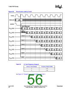
However, for a synchronous non-array read, the same word of data will be output on successive
clock edges until the burst length requirements are satisfied. Refer to the following waveforms for
more detailed information:
• Figure 19, “Synchronous Single-Word Array or Non-array Read Timing” on page 39
• Figure 20, “Continuous Burst Read, showing an Output Delay Timing” on page 40
• Figure 21, “Synchronous Burst-Mode Four-Word Read Timing” on page 41
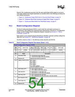
10.3
Read Configuration Register
The Read Configuration Register (RCR) is used to select the read mode (synchronous or
asynchronous), and it defines the synchronous burst characteristics of the device. To modify RCR
settings, use the Configure Read Configuration Register command (see Section 9.2, “Device
Commands” on page 50).
RCR contents can be examined using the Read Device Identifier command, and then reading from
offset 0x05 (see Section 14.2, “Read Device Identifier” on page 76).
The RCR is shown in Table 22. The following sections describe each RCR bit.
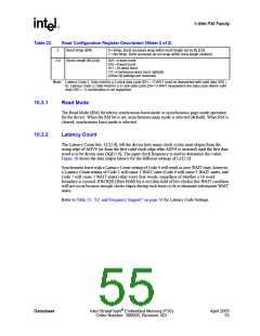
Table 22.
Read Configuration Register Description (Sheet 1 of 2)
Read Configuration Register (RCR)
Data WAIT
Hold Delay
Burst
Wrap
Read
Mode
WAIT
Burst
Seq
CLK
RES
Latency Count
LC[2:0]
RES RES
Burst Length
Polarity
Edge
RM
15
R
WP
10
DH
9
WD
8
BS
7
CE
6
R
5
R
4
BW
3
BL[2:0]
1
14
13
12
11
2
0
Bit
15
Name
Description
Read Mode (RM)
Reserved (R)
0 = Synchronous burst-mode read
1 = Asynchronous page-mode read (default)
Reserved bits should be cleared (0)
14
13:11 Latency Count (LC[2:0])
010 =Code 2
011 =Code 3
100 =Code 4
101 =Code 5
110 =Code 6
111 =Code 7 (default)
(Other bit settings are reserved)
10
9
Wait Polarity (WP)
Data Hold (DH)
0 =WAIT signal is active low
1 =WAIT signal is active high (default)
0 =Data held for a 1-clock data cycle
1 =Data held for a 2-clock data cycle (default)
8
Wait Delay (WD)
Burst Sequence (BS)
Clock Edge (CE)
Reserved (R)
0 =WAIT deasserted with valid data
1 =WAIT deasserted one data cycle before valid data (default)
7
0 =Reserved
1 =Linear (default)
6
0 = Falling edge
1 = Rising edge (default)
5:4
Reserved bits should be cleared (0)
April 2005
54
Intel StrataFlash® Embedded Memory (P30)
Order Number: 306666, Revision: 001
Datasheet

 INTEL [ INTEL ]