1-Gbit P30 Family
Table 18.
AC Write Specifications (Sheet 2 of 2)
Num
Symbol
Parameter
WE# high to OE# low
WE# high to read valid
Min
Max
Units
Notes
W14 tWHGL
W16 tWHQV
0
-
ns
1,2,9
1,2,3,6,1
0
t
+ 35
-
ns
AVQV
Write to Asynchronous Read Specifications
W18 tWHAV WE# high to Address valid
Write to Synchronous Read Specifications
0
-
ns
1,2,3,6,8
W19 tWHCH/L
W20 tWHVH
WE# high to Clock valid
WE# high to ADV# high
19
19
-
-
ns
ns
1,2,3,6,1
0
Write Specifications with Clock Active
W21 tVHWL
W22 tCHWL
Notes:
ADV# high to WE# low
Clock high to WE# low
-
-
20
20
ns
ns
1,2,3,11
1.
2.
3.
4.
Write timing characteristics during erase suspend are the same as write-only operations.
A write operation can be terminated with either CE# or WE#.
Sampled, not 100% tested.
Write pulse width low (t
or t
) is defined from CE# or WE# low (whichever occurs last) to
WLWH
ELEH
CE# or WE# high (whichever occurs first). Hence, t
= t
= t
= t
.
ELWH
WLWH
ELEH
WLEH
5.
Write pulse width high (t
or t
) is defined from CE# or WE# high (whichever occurs first) to
WHWL
EHEL
CE# or WE# low (whichever occurs last). Hence, t
= t
= t
= t
).
EHWL
WHWL
EHEL
WHEL
6.
7.
8.
tWHVH or tWHCH/L must be met when transitioning from a write cycle to a synchronous burst read.
V
and WP# should be at a valid level until erase or program success is determined.
PP
This specification is only applicable when transitioning from a write cycle to an asynchronous read.
See spec W19 and W20 for synchronous read.
9.
When doing a Read Status operation following any command that alters the Status Register, W14 is
20 ns.
10.
11.
Add 10 ns if the write operations results in a RCR or block lock status change, for the subsequent
read operation to reflect this change.
These specs are required only when the device is in a synchronous mode and clock is active during
address setup phase.
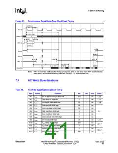
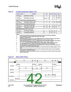
Figure 22.
Write-to-Write Timing
W5
W8
W5
W8
Address [A]
CE# [E}
W2
W6
W2
W6
W3
W9
W3
WE# [W]
OE# [G]
W4
W7
W4
W7
Data [D/Q]
RST# [P]
W1
April 2005
42
Intel StrataFlash® Embedded Memory (P30)
Order Number: 306666, Revision: 001
Datasheet

 INTEL [ INTEL ]