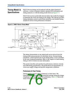
Timing Model & Specifications
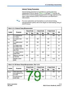
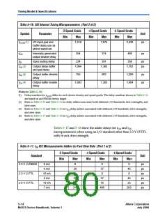
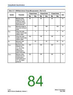
Table 5–16. IOE Internal Timing Microparameters (Part 2 of 2)
-3 Speed Grade
-4 Speed Grade
-5 Speed Grade
Symbol
Parameter
Unit
Min
Max
Min
Max
Min
Max
tGLOB (1)
I/O input pad and
buffer delay use as
global signal pin
1,519
1,974
2,430
ps
tIOE
Internally generated
output enable delay
354
374
460
ps
tDL
Input routing delay
224
291
358
ps
ps
tOD (2)
Output delay buffer
and pad delay
1,064
1,383
1,702
tXZ (3)
tZX (4)
Output buffer disable
delay
756
982
1,209
1,604
ps
ps
Output buffer enable
delay
1,003
1,303
Notes to Table 5–16:
(1) Delay numbers for tGLOB differ for each device density and speed grade. The delay numbers shown in Table 5–16
are based on an EPM240 device target.
(2) Refer to Table 5–29 and Table 5–31 for delay adders associated with different I/O Standards, drive strengths, and
slew rates.
(3) Refer to Table 5–19 and Table 5–20 for tXZ delay adders associated with different I/O Standards, drive strengths,
and slew rates.
(4) Refer to Table 5–17 and Table 5–18 for tZX delay adders associated with different I/O Standards, drive strengths,
and slew rates.
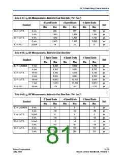
Tables 5–17 and 5–18 show the adder delays for tOD and tZX
microparameters when using an I/O standard other than 3.3-V LVTTL
with 16 mA drive strength.
Table 5–17. tZX IOE Microparameter Adders for Fast Slew Rate (Part 1 of 2)
-3 Speed Grade
-4 Speed Grade
-5 Speed Grade
Standard
Unit
Min
Max
Min
Max
Min
Max
3.3-V LVCMOS
8 mA
4 mA
16 mA
8 mA
14 mA
7 mA
0
28
0
0
37
0
0
45
0
ps
ps
ps
ps
ps
ps
3.3-V LVTTL
2.5-V LVTTL
28
14
314
37
19
409
45
23
503
5–14
Core Version a.b.c variable
Altera Corporation
July 2006
MAX II Device Handbook, Volume 1

 INTEL [ INTEL ]