®
MOBILE PENTIUM PROCESSOR WITH MMX™ TECHNOLOGY
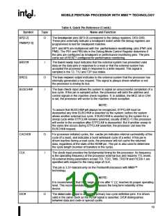
PCHK#
PEN#
O
I
The parity check output indicates the result of a parity check on a data read. It is
driven with parity status two clocks after BRDY# is returned. PCHK# remains low
one clock for each clock in which a parity error was detected. Parity is checked
only for the bytes on which valid data is returned.
The parity enable input (along with CR4.MCE) determines whether a machine
check exception will be taken as a result of a data parity error on a read cycle. If
this pin is sampled active in the clock, a data parity error is detected. The
processor will latch the address and control signals of the cycle with the parity
error in the machine check registers. If, in addition, the machine check enable bit
in CR4 is set to "1", the processor will vector to the machine check exception
before the beginning of the next instruction.
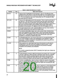
PICCLK
I
The APIC interrupt controller serial data bus clock is driven into the
programmable interrupt controller clock input of the Pentium processor with
®
MMX™ technology.
PICD0-1
I/O
Programmable interrupt controller data lines 0-1 of the Pentium® processor
with MMX™ technology comprise the data portion of the APIC 3-wire bus. They
are open-drain outputs that require external pull-up resistor. These signals are
multiplexed with APICEN.
[APICEN]
PM/BP[1:0]
O
These pins function as part of the performance monitoring feature.
The breakpoint 1-0 pins are multiplexed with the performance monitoring 1 -0
pins. The PB1 and PB0 bits in the Debug Mode Control Register determine if the
pins are configured as breakpoint or performance monitoring pins. The pins come
out of RESET configured for performance monitoring.
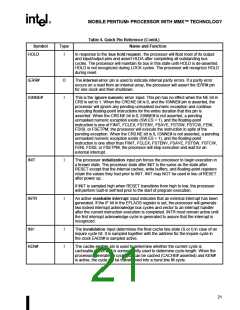
PRDY
PWT
O
O
The probe ready output pin indicates that the processor has stopped normal
execution in response to the R/S# pin going active or Probe Mode being entered.
The page writethrough pin reflects the state of the PWT bit in CR3, the page
directory entry, or the page table entry. The PWT pin is used to provide an
external writeback indication on a page-by-page basis.
23

 INTEL [ INTEL ]