®
MOBILE PENTIUM PROCESSOR WITH MMX™ TECHNOLOGY
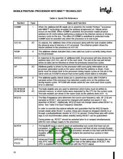
Table 4. Quick Pin Reference (Contd.)
Name and Function
Symbol
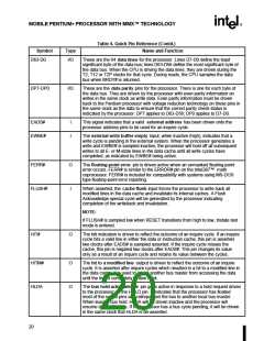
BP[3:2]
Type
O
The breakpoint pins (BP3-0) correspond to the debug registers, DR3-DR0.
These pins externally indicate a breakpoint match when the debug registers are
programmed to test for breakpoint matches.
PM/BP[1:0]
BP1 and BP0 are multiplexed with the performance monitoring pins (PM1 and
PM0). The PB1 and PB0 bits in the Debug Mode Control Register determine if
the pins are configured as breakpoint or performance monitoring pins. The pins
come out of RESET configured for performance monitoring.
BRDY#
I
The burst ready input indicates that the external system has presented valid
data on the data pins in response to a read or that the external system has
accepted the processor data in response to a write request. This signal is
sampled in the T2, T12 and T2P bus states.
BREQ
O
I
The bus request output indicates to the external system that the processor has
internally generated a bus request. This signal is always driven whether or not
the processor is driving its bus.
BUSCHK#
The bus check input allows the system to signal an unsuccessful completion of a
bus cycle. If this pin is sampled active, the processor will latch the address and
control signals in the machine check registers. If, in addition, the MCE bit in CR4
is set, the processor will vector to the machine check exception.
NOTE:
To assure that BUSCHK# will always be recognized, STPCLK# must be
deasserted any time BUSCHK# is asserted by the system, before the system
allows another external bus cycle. If BUSCHK# is asserted by the system for a
snoop cycle while STPCLK# remains asserted, usually (if MCE=1) the processor
will vector to the exception after STPCLK# is deasserted. But if another snoop to
the same line occurs during STPCLK# assertion, the processor can lose the
BUSCHK# request.
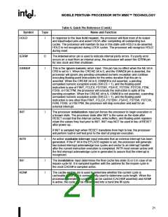
CACHE#
CLK
O
I
For processor-initiated cycles, the cache pin indicates internal cacheability of the
cycle (if a read), and indicates a burst writeback cycle (if a write). If this pin is
driven inactive during a read cycle, the processor will not cache the returned
data, regardless of the state of the KEN# pin. This pin is also used to determine
the cycle length (number of transfers in the cycle).
The clock input provides the fundamental timing for the processor. Its frequency
is the operating frequency of the processor external bus and requires TTL levels.
All external timing parameters except TDI, TDO, TMS, TRST# and PICD0-1 are
specified with respect to the rising edge of CLK.
This pin is 3.3V-tolerant-only on the Pentium® processor with MMX™
technology.
NOTE:
It is recommended that CLK begin 150 ms after V
level. This recommendation is only to assure the long term reliability of the
device.
reaches its proper operating
CC
D/C#
O
The data/code output is one of the primary bus cycle definition pins. It is driven
valid in the same clock as the ADS# signal is asserted. D/C# distinguishes
between data and code or special cycles.
19

 INTEL [ INTEL ]