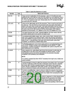
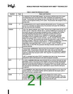
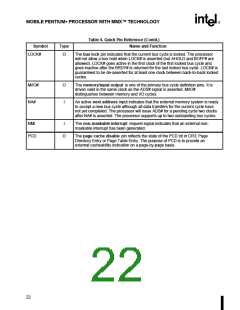
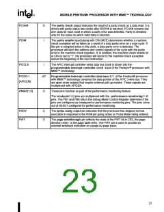
®
MOBILE PENTIUM PROCESSOR WITH MMX™ TECHNOLOGY
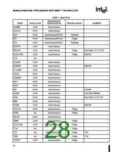
Table 4. Quick Pin Reference (Contd.)
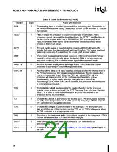
Symbol
R/S#
Type
Name and Function
I
The run/stop input is provided for use with the Intel debug port. Please refer to
the Pentium Processor Family Developer’s Manual (Order Number 241428) for
®
more details.
RESET
I
RESET forces the processor to begin execution at a known state. All the
processor internal caches will be invalidated upon the RESET. Modified lines in
the data cache are not written back. FLUSH# and INIT are sampled when
RESET transitions from high to low to determine if tristate test mode will be
entered or if BIST will be run.
SCYC
SMI#
O
I
The split cycle output is asserted during misaligned LOCKed transfers to
indicate that more than two cycles will be locked together. This signal is defined
for locked cycles only. It is undefined for cycles which are not locked.
The system management interrupt causes a system management interrupt
request to be latched internally. When the latched SMI# is recognized on an
instruction boundary, the processor enters System Management Mode.
SMIACT#
STPCLK#
O
I
An active system management interrupt active output indicates that the
processor is operating in System Management Mode.
Assertion of the stop clock input signifies a request to stop the internal clock of
the Pentium processor with voltage reduction technology thereby causing the
core to consume less power. When the CPU recognizes STPCLK#, the
processor will stop execution on the next instruction boundary, unless
superseded by a higher priority interrupt, and generate a Stop Grant
Acknowledge cycle. When STPCLK# is asserted, the processor will still respond
to external snoop requests.
TCK
I
The testability clock input provides the clocking function for the processor
boundary scan in accordance with the IEEE Boundary Scan interface (Standard
1149.1). It is used to clock state information and data into and out of the
processor during boundary scan.
TDI
I
The test data input is a serial input for the test logic. TAP instructions and data
are shifted into the processor on the TDI pin on the rising edge of TCK when the
TAP controller is in an appropriate state.
TDO
O
The test data output is a serial output of the test logic. TAP instructions and
data are shifted out of the processor on the TDO pin on TCK's falling edge when
the TAP controller is in an appropriate state.
TMS
I
I
I
The value of the test mode select input signal sampled at the rising edge of TCK
controls the sequence of TAP controller state changes.
TRST#
VCC2
When asserted, the test reset input allows the TAP controller to be
asynchronously initialized.
These pins are the 1.8V (166/200/233 MHz) or 2.0V (266 MHz) power inputs to
the core.
24

 INTEL [ INTEL ]