®
MOBILE PENTIUM PROCESSOR WITH MMX™ TECHNOLOGY
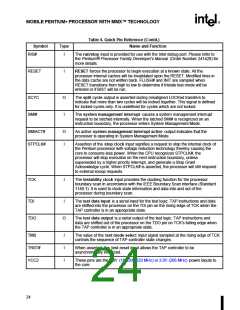
Table 4. Quick Pin Reference (Contd.)
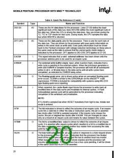
Symbol
D63-D0
Type
Name and Function
I/O
These are the 64 data lines for the processor. Lines D7-D0 define the least
significant byte of the data bus; lines D63-D56 define the most significant byte of
the data bus. When the CPU is driving the data lines, they are driven during the
T2, T12 or T2P clocks for that cycle. During reads, the CPU samples the data
bus when BRDY# is returned.
DP7-DP0
I/O
These are the data parity pins for the processor. There is one for each byte of
the data bus. They are driven by the processor with even parity information on
writes in the same clock as write data. Even parity information must be driven
back to the Pentium processor with voltage reduction technology on these pins in
the same clock as the data to ensure that the correct parity check status is
indicated by the processor. DP7 applies to D63-D56; DP0 applies to D7-D0.
EADS#
EWBE#
I
I
This signal indicates that a valid external address has been driven onto the
processor address pins to be used for an inquire cycle.
The external write buffer empty input, when inactive (high), indicates that a
write cycle is pending in the external system. When the processor generates a
write and EWBE# is sampled inactive, the processor will hold off all subsequent
writes to all E- or M-state lines in the data cache until all write cycles have
completed, as indicated by EWBE# being active.
FERR#
O
I
The floating-point error pin is driven active when an unmasked floating-point
error occurs. FERR# is similar to the ERROR# pin on the Intel387™ math
coprocessor. FERR# is included for compatibility with systems using MS-DOS
type floating-point error reporting.
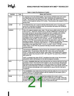
FLUSH#
When asserted, the cache flush input forces the processor to write back all
modified lines in the data cache and invalidate its internal caches. A Flush
Acknowledge special cycle will be generated by the processor indicating
completion of the writeback and invalidation.
NOTE:
If FLUSH# is sampled low when RESET transitions from high to low, tristate test
mode is entered.
HIT#
O
The hit indication is driven to reflect the outcome of an inquire cycle. If an inquire
cycle hits a valid line in either the data or instruction cache, this pin is asserted
two clocks after EADS# is sampled asserted. If the inquire cycle misses the
cache, this pin is negated two clocks after EADS#. This pin changes its value
only as a result of an inquire cycle and retains its value between the cycles.
HITM#
HLDA
O
O
The hit to a modified line output is driven to reflect the outcome of an inquire
cycle. It is asserted after inquire cycles which resulted in a hit to a modified line in
the data cache. It is used to inhibit another bus master from accessing the data
until the line is completely written back.
The bus hold acknowledge pin goes active in response to a hold request driven
to the processor on the HOLD pin. It indicates that the processor has floated
most of the output pins and relinquished the bus to another local bus master.
When leaving bus hold, HLDA will be driven inactive and the processor will
resume driving the bus. If the processor has a bus cycle pending, it will be driven
in the same clock that HLDA is de-asserted.
20

 INTEL [ INTEL ]