®
MOBILE PENTIUM PROCESSOR WITH MMX™ TECHNOLOGY
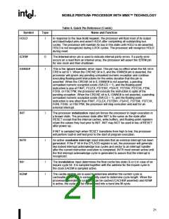
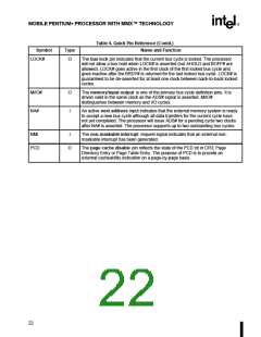
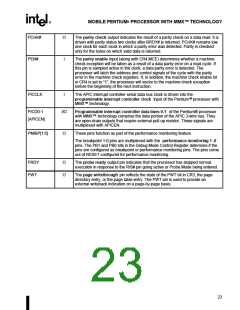
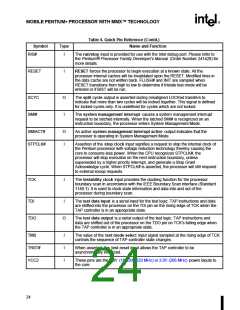
Table 4. Quick Pin Reference (Contd.)
Name and Function
Symbol
VCC3
Type
I
I
These pins are the 2.5V power inputs to the I/O.
These pins are the ground inputs.
VSS
W/R#
O
Write/read is one of the primary bus cycle definition pins. It is driven valid in the
same clock as the ADS# signal is asserted. W/R# distinguishes between write
and read cycles.
WB/WT#
I
The writeback/writethrough input allows a data cache line to be defined as
writeback or writethrough on a line-by-line basis. As a result, it determines
whether a cache line is initially in the S or E state in the data cache.
25

 INTEL [ INTEL ]