®
MOBILE PENTIUM PROCESSOR WITH MMX™ TECHNOLOGY
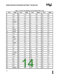
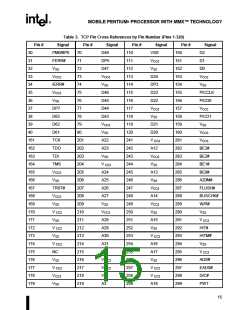
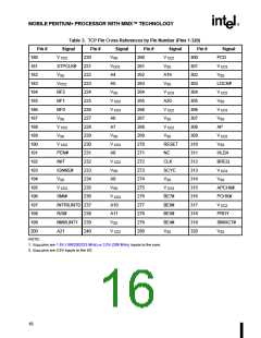
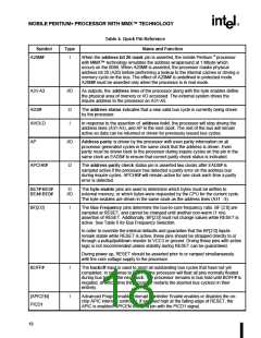
Table 4. Quick Pin Reference
Symbol
A20M#
Type
Name and Function
I
When the address bit 20 mask pin is asserted, the mobile Pentium ® processor
with MMX™ technology emulates the address wraparound at 1 Mbyte which
occurs on the 8086. When A20M# is asserted, the processor masks physical
address bit 20 (A20) before performing a lookup to the internal caches or driving a
memory cycle on the bus. The effect of A20M# is undefined in protected mode.
A20M# must be asserted only when the processor is in real mode.
A31-A3
I/O
As outputs, the address lines of the processor along with the byte enables define
the physical area of memory or I/O accessed. The external system drives the
inquire address to the processor on A31-A5.
ADS#
O
I
The address status indicates that a new valid bus cycle is currently being driven
by the processor.
AHOLD
In response to the assertion of address hold, the processor will stop driving the
address lines (A31-A3), and AP in the next clock. The rest of the bus will remain
active so data can be returned or driven for previously issued bus cycles.
AP
I/O
O
Address parity is driven by the processor with even parity information on all
processor generated cycles in the same clock that the address is driven. Even
parity must be driven back to the processor during inquire cycles on this pin in the
same clock as EADS# to ensure that correct parity check status is indicated.
APCHK#
The address parity check status pin is asserted two clocks after EADS# is
sampled active if the processor has detected a parity error on the address bus
during inquire cycles. APCHK# will remain active for one clock each time a parity
error is detected.
BE7#-BE5#
BE4#-BE0#
O
I/O
The byte enable pins are used to determine which bytes must be written to
external memory, or which bytes were requested by the CPU for the current cycle.
The byte enables are driven in the same clock as the address lines (A31 -3).
BF[2:0]
I
The Bus Frequency pins determine the bus-to-core frequency ratio. BF [2:0] are
sampled at RESET, and cannot be changed until another non-warm (1 ms)
assertion of RESET. Additionally, BF[2:0] must not change values while RESET is
active. See Table 6 for Bus Frequency Selection.
In order to override the internal defaults and guarantee that the BF[2:0] inputs
remain stable while RESET is active, these pins should be strapped directly to or
through a pullup/pulldown resistor to VCC3 or ground. Drving these pins with active
logic is not recommended unless stability during RESET can be guaranteed.
During power up, RESET should be asserted prior to or ramped simultaneously
with the core voltage supply to the processor.
BOFF#
I
I
The backoff input is used to abort all outstanding bus cycles that have not yet
completed. In response to BOFF#, the processor will float all pins normally floated
during bus hold in the next clock. The processor remains in bus hold until BOFF# is
negated, at which time the processor restarts the aborted bus cycle(s) in their
entirety.
[APICEN]
PICD1
Advanced Programmable Interrupt Controller Enable enables or disables the on-
chip APIC interrupt controller. If sampled high at the falling edge of RESET, the
APIC is enabled. APICEN shares a pin with the PICD1 signal.
18

 INTEL [ INTEL ]