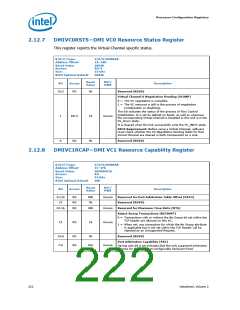
Processor Configuration Registers
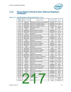
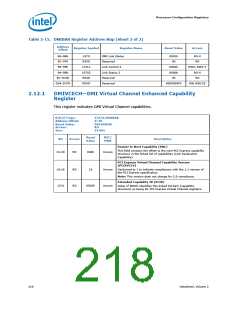
Table 2-15. DMIBAR Register Address Map (Sheet 2 of 2)
Address
Offset
Register Symbol
Register Name
Reset Value
Access
8A–8Bh
8C–97h
LSTS
RSVD
LCTL2
LSTS2
RSVD
RSVD
DMI Link Status
0001h
0h
RO-V
RO
Reserved
98–99h
Link Control 2
Link Status 2
Reserved
0002h
0000h
0h
RWS, RWS-V
RO-V
9A–9Bh
9C–D33h
D34–D37h
RO
Reserved
0000005Fh
RW, RW1CS
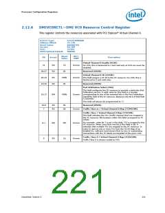
2.12.1
DMIVCECH—DMI Virtual Channel Enhanced Capability
Register
This register indicates DMI Virtual Channel capabilities.
B/D/F/Type:
Address Offset:
Reset Value:
Access:
0/0/0/DMIBAR
0–3h
04010002h
RO
32 bits
Size:
Reset
Value
RST/
PWR
Bit
Access
Description
Pointer to Next Capability (PNC)
This field contains the offset to the next PCI Express capability
structure in the linked list of capabilities (Link Declaration
Capability).
31:20
RO
040h
Uncore
PCI Express Virtual Channel Capability Version
(PCIEVCCV)
19:16
15:0
RO
RO
1h
Uncore
Uncore
Hardwired to 1 to indicate compliances with the 1.1 version of
the PCI Express specification.
Note: This version does not change for 2.0 compliance.
Extended Capability ID (ECID)
Value of 0002h identifies this linked list item (capability
structure) as being for PCI Express Virtual Channel registers.
0002h
218
Datasheet, Volume 2

 INTEL [ INTEL ]