Processor Configuration Registers
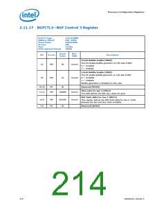
2.11.17 BGFCTL3—BGF Control 3 Register
B/D/F/Type:
Address Offset:
Reset Value:
Access:
0/6/0/MMR
D6C–D6Fh
400204E0h
RW
Size:
32 bits
BIOS Optimal Default
0000h
Reset
Value
RST/
PWR
Bit
Access
Description
Fclock Bubble Enable (FBEN)
This bit disable Bubble generator on Fclk side of BGF.
0 = Disabled
1 = Enabled.
31
RW
0b
Uncore
Uncore
Lclock Bubble Enable (LBEN)
This bit enable Bubble generator on Lclk side of BGF
0 = Disabled
1 = Enabled.
Bubble generation is disabled on slow side
30
RW
1b
0h
29:18
17:13
RO
Reserved (RSVD)
Slow ratio for gen 3 (SRG3)
This field defines the BGF slow ration for gen3
RW
10000b
Uncore
Uncore
BGF Ratio delta for Gen 3 (RDG3)
This register defines the BGF Ratio delta for Gen 3. Delta
between the fast and slow clock multiplier
12:8
7:0
RW
RO
00100b
0h
Reserved (RSVD)
214
Datasheet, Volume 2

 INTEL [ INTEL ]