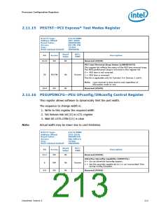
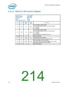
Processor Configuration Registers
2.11.9
LE1D—Link Entry 1 Description Register
This register provides the first part of a Link Entry that declares an internal link to
another Root Complex Element.
B/D/F/Type:
Address Offset:
Reset Value:
Access:
0/6/0/MMR
150–153h
00000000h
RO, RW-O
32 bits
Size:
BIOS Optimal Default
0000h
Reset
Value
RST/
PWR
Bit
Access
Description
Target Port Number (TPN)
Specifies the port number associated with the element targeted
by this link entry (Egress Port). The target port number is with
respect to the component that contains this element as specified
by the target component ID.
31:24
RO
00h
00h
Uncore
Uncore
00h is the egress port (memory).
Target Component ID (TCID)
Identifies the physical or logical component that is targeted by
this link entry.
BIOS Requirement: This field must be initialized according to
guidelines in the PCI Express* Isochronous/Virtual Channel
Support Hardware Programming Specification (HPS).
23:16
RW-O
15:2
1
RO
RO
0h
0b
Reserved (RSVD)
Link Type (LTYP)
Indicates that the link points to memory-mapped space (for
RCRB). The link address specifies the 64-bit base address of the
target RCRB.
Uncore
Uncore
Link Valid (LV)
0 = Link Entry is not valid and will be ignored.
1 = Link Entry specifies a valid link.
BIOS should write "1' to this bit once it has programmed Link
Entry 1 Address (LE1A) and while it writes the TCID in this
register
0
RW-O
0b
2.11.10 LE1A—Link Entry 1 Address Register
This register provides the second part of a Link Entry that declares an internal link to
another Root Complex Element.
B/D/F/Type:
Address Offset:
Reset Value:
Access:
0/6/0/MMR
158–15Bh
00000000h
RW-O
32 bits
000h
Size:
BIOS Optimal Default
Reset
Value
RST/
PWR
Bit
Access
Description
Link Address (LA)
Memory mapped base address of the RCRB that is the target
element (Egress Port) for this link entry.
BIOS Requirement: This field is inserted by BIOS such that it
matches PXPEPBAR.
31:12
11:0
RW-O
RO
00000h
0h
Uncore
Reserved (RSVD)
210
Datasheet, Volume 2

 INTEL [ INTEL ]