Processor Configuration Registers
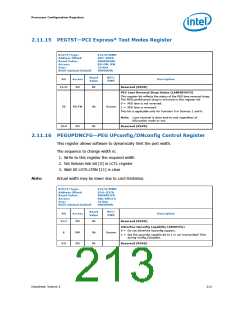
2.11.15 PEGTST—PCI Express* Test Modes Register
B/D/F/Type:
Address Offset:
Reset Value:
Access:
0/6/0/MMR
D0C–D0Fh
00000000h
RO-FW, RW
32 bits
Size:
BIOS Optimal Default
0000000h
Reset
Value
RST/
PWR
Bit
Access
Description
31:21
RO
0h
0b
0h
Reserved (RSVD)
PEG Lane Reversal Strap Status (LANEREVSTS)
This register bit reflects the status of the PEG lane reversal strap.
The PEGLaneReversal strap is mirrored in this register bit.
0 = PEG lane is not reversed.
1 = PEG lane is reversed.
20
RO-FW
RO
Uncore
This bit is applicable only for Function 0 in Devices 1 and 6.
Note: Lane reversal is done end-to-end regardless of
bifurcation mode or not.
19:0
Reserved (RSVD)
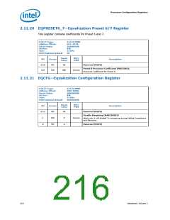
2.11.16 PEGUPDNCFG—PEG UPconfig/DNconfig Control Register
This register allows software to dynamically limit the port width.
The sequence to change width is:
1. Write to this register the required width
2. Set Retrain link bit [5] in LCTL register
3. Wait till LSTS.LTRN [11] is clear
Note:
Actual width may be lower due to card limitation.
B/D/F/Type:
Address Offset:
Reset Value:
Access:
0/6/0/MMR
D34–D37h
0000001Fh
RW, RW1CS
32 bits
Size:
BIOS Optimal Default
0000000h
Reset
Value
RST/
PWR
Bit
Access
Description
31:7
RO
0h
0b
0h
Reserved (RSVD)
Advertise Upconfig Capability (ADUPCFG)
0 = Do not advertise Upconfig support.
1 = Set the upconfig capable bit to 1 in our transmitted TS2s
during Config.Complete.
6
RW
RO
Uncore
5:0
Reserved (RSVD)
Datasheet, Volume 2
213

 INTEL [ INTEL ]