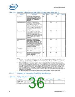
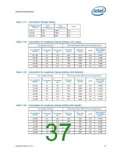
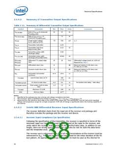
Electrical Specifications
Table 2-22. Summary of Differential Receiver Input Specifications (Sheet 2 of 2)
Symbol
Parameter
Min
Max
Units
Comments
V
V
Common mode of the input voltage
(Absolute max)
375
mV
V
V
DC
of |V
+ V
|/2
RX-D-
RX-CM-ABS
RX-CM =
(avg)
RX-D+
AC peak-to-peak common mode of
input voltage
270
45
mV
=
RX-CM-ACp-p
RX-CM-AC
Max |V
Min |V
Measured as: Note 1
+ V
+ V
|/2–
RX-D+
RX-D-
|/2
RX-D-
RX-D+
V
Ratio of V
to minimum
%
11
RX-CM-AC-EH-Ratio
RX-CM-ACp-p
RX-DIFFp-p
V
RL
Differential return loss
9
6
dB
Measured over 0.1GHz to 3.2 GHz.
See also Note 12
RX-DIFF
RX-CM
RL
Common mode return loss
dB
Measured over 0.1GHz to 3.2 GHz.
See also Note 12
R
RX termination resistance
37.4
0.0
47.6
1.0
Ohm
ns
RX
T
T
T
RX skew between clock and data
Forwarded clock delay - data delay
14
RX-SKEW-CLK-DATA
Minimum RX Drift Tolerance
Fast reset entry detect time
Bit Error Ratio
600
ps
UI
RX-DRIFT
240
FR-ENTRY -DETECT
-12
10
BER
Notes:
1.
2.
3.
4.
Specified at the package pins into a timing and voltage compliant test setup.
The V pin specification reflects a target eye height at the pad equal to 70 mV.
RX-DIFFp-p
Specified at the package pins into a timing and voltage compliance test setup.
The single-pulse mask provides sufficient symbol energy for reliable RX reception. Each symbol must comply with both the
single-pulse mask and the cumulative eye mask.
The relative amplitude ratio limit between adjacent symbols prevents excessive inter-symbol interference in the Rx. Each
symbol must comply with the peak amplitude ratio with regard to both the preceding and subsequent symbols.
This number does not include the effects of SSC or reference clock jitter.
5.
6.
7.
8.
9.
The T
The T
pin specification reflects a target eye width at the pad equal to 0.45 UI.
RX-Eye-MIN
pin specification reflects a target max deterministic jitter at the pad equal to 0.45 UI.
RX-DJ-DD
Defined as the dual-dirac deterministic jitter at the receiver input.
10. Allows for 15 mV DC offset between transmit and receive devices.
11. The received differential signal must satisfy both this ratio as well as the absolute maximum AC peak-to-peak common mode
specification. For example, if V
is 200 mV, the maximum AC peak-to-peak common mode is the lesser of
RX-CM-ACp-p
RX-DIFFp-p
(200 mV * 0.45 = 90 mV) and V
.
12. One of the components that contribute to the deterioration of the return loss is the ESD structure which needs to be carefully
designed.
13. The termination small signal resistance; tolerance over the entire signaling voltage range shall not exceed ± 5 Ω.
14. Measured from the reference clock edge to the center of the input eye. This specification must be met across specified voltage
and temperature ranges for a single component. Drift rate of change is significantly below the tracking capability of the
receiver.
2.6
Platform Environmental Control Interface (PECI)
DC Specifications
PECI is an Intel proprietary interface that provides a communication channel between
Intel processors and chipset components to external thermal monitoring devices. The
Intel Xeon Processor E7-8800/4800/2800 Product Families processor contains a Digital
Thermal Sensor (DTS) that reports a relative die temperature as an offset from TCC
40
Datasheet Volume 1 of 2

 INTEL [ INTEL ]