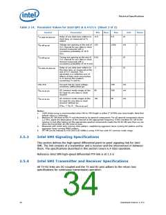
Electrical Specifications
2.5.4.2
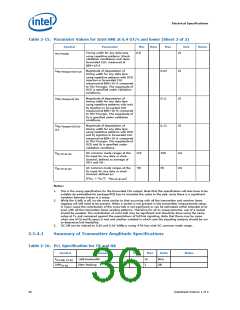
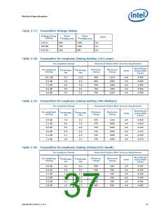
Summary of Transmitter Output Specifications
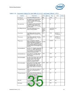
Table 2-21. Summary of Differential Transmitter Output Specifications
Symbol
Parameter
Min
Max
Units
Comments
V
V
V
Ratio of V
TX-DIFFp-p (DC)
to measured
23
27
%
TX-CM-Ratio
TX-CM
V
Ratio of V
measured V
to
7.5
%
TX-CM-AC-Ratio
TX-SE
TX-CM-ACp-p
TX-DIFFp-p (DC)
Single-ended voltage
(w.r.t. VSS) on D+/D-
-75
750
mV
1, 2
T
T
Transmitter total jitter
0.25
0.15
TX_TJ
Transmitter dual-dirac
deterministic jitter
UI
TX_DJ
T
T
Transmitter pulse width
shrinkage (data)
0.05
0.018
30
TX_PWS
Transmitter pulse width
shrinkage (forwarded clock)
UI
TX_CLK_PWS
ER
ER
,
Differential TX output edge
rates
10
V/ns
Differential voltage levels at ±100 mV
Measured as: Note 1
TX-RISE
TX-FALL
RL
Differential return loss
8
6
dB
dB
Ω
Measured relative to 50 ohms over
0.1 GHz to 3.2 GHz.
TX-DIFF
RL
Common mode return loss
Measured relative to 50 ohms over
0.1 GHz to 3.2 GHz.
TX-CM
R
Transmitter termination
resistance
37.4
47.6
TX
L
Lane-to-lane skew at TX
100
ps
TX-SKEW
+ 2 UI
L
TX clock-to-data skew
-0.2
-1.5
0.2
1.5
ns
ns
Forwarded clock delay - data delay
TX-SKEW-CLK-DAT
L
Total system clock-to-data
skew
TOT-SKEW-CLK-DAT
T
Maximum TX Drift
Bit Error Ratio
240
ps
3
TX-DRIFT
-12
10
BER
Notes:
1.
2.
3.
Specified at the package pins into a timing and voltage compliance test load.
The maximum value is specified to be at least (V / 4) + V + (V / 2)
TX-CM-ACp-p
Measured from the reference clock edge to the center of the output eye. This specification must be met across specified
voltage and temperature ranges for a single component. Drift rate of change is significantly below the tracking capability of
the receiver.
TX-DIFFp-p L
TX-CM L
2.5.4.3
Intel® SMI Differential Receiver Input Specifications
The receiver definition starts from the input pin of the receiver end package and
therefore includes the package and the receiver end device.
2.5.4.3.1
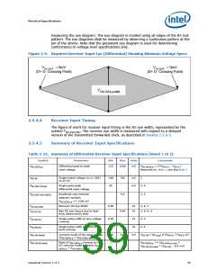
Receiver Input Compliance Eye Specification
Following the specification of the transmitter, the receiver is specified in terms of the
minimum input eye height that must be maintained at the input to the receiver, and
under which the receiver must function at the specified data rates. In addition to eye
height, there are timing specifications that must also be met for both the data lanes
and the forwarded clock.
The receiver eye is referenced to VSS and all input terminations at the receiver must be
referenced to VSS. This input eye must be maintained for the entire duration of the RX
test pattern. An appropriate average transmitter UI must be used as the interval for
38
Datasheet Volume 1 of 2

 INTEL [ INTEL ]