Electrical Specifications
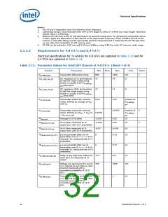
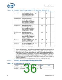
Table 2-15. Parameter Values for Intel SMI at 6.4 GT/s and lower (Sheet 2 of 2)
Symbol
Parameter
Min
0.8
Nom
Max
Unit
Notes
Timing width for any data lane
using repetitive patterns (check
validation conditions) and clean
forwarded CLK, measured at
BER=1E-9
UI
UI
TRx-Tmargin
Δ
Δ
Δ
Magnitude of degradation of
timing width for any data lane
using repetitive patterns with DCD
injection in forwarded CLK
measured at BER=1E-9, compared
to TRx-Tmargin. The magnitude of
DCD is specified under validation
conditions.
0.02
TRx-Tmargin-DCD-CLK
TRx-Tmargin-Rj-CLK
TRx-Tmargin-DCD-Rj-
Magnitude of degradation of
timing width for any data lane
using repetitive patterns with only
Rj injection in forwarded CLK
measured at BER=1E-9, compared
to TRx-Tmargin. The magnitude of
Rj is specified under validation
conditions.
0.11
0.12
UI
UI
Magnitude of degradation of
timing width for any data lane
using repetitive patterns with DCD
and Rj injection in forwarded CLK
measured at BER=1E-9, compared
to TRx-Tmargin. The magnitude of
DCD and Rj is specified under
validation conditions.
CLK
V
V
DC common mode ranges at the
Rx input for any data or clock
channel, defined as average of
VD+ and VD-.
125
-50
350
50
mV
mV
Rx-cm-dc-pin
Rx-cm-ac-pin
AC common mode ranges at the
Rx input for any data or clock
channel, defined as:
((V
+ V /2 - V
)
RX-cm-dc-pin
D+
D-
Notes:
1.
This is the swing specification for the forwarded CLK output. Note that this specification will also have to be
suitably de-embedded for package/PCB loss to translate the value to the pad, since there is a significant
variation between traces in a setup.
2.
While the X-talk is off, on-die noise similar to that occurring with all the transmitter and receiver lanes
toggling will still need to be present. When a socket is not present in the transmitter measurement setup,
in many cases the contribution of the cross-talk is not significant or can be estimated within tolerable error
even with all the transmitter lanes sending patterns. Therefore for all Tx measurements, use of a socket
should be avoided. The contribution of cross-talk may be significant and should be done using the same
setup at Tx and compared against the expectations of full link signaling. Note that there may be cases
when one of Dj and Rj specs is met and another violated in which case the signaling analysis should be run
to determine link feasibility.
3.
DC CM can be relaxed to 0.20 and 0.30 Vdiffp-p swing if RX has wide DC common mode range.
2.5.4.1
Summary of Transmitter Amplitude Specifications
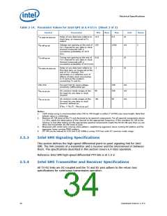
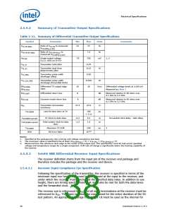
Table 2-16. PLL Specification for TX and RX
Symbol
Parameter
Min
Max
16
Units
Notes
F
-3dB bandwidth
Jitter Peaking
4
MHz
dB
PLL-BW_TX-RX
JitPk
3
TX-RX
36
Datasheet Volume 1 of 2

 INTEL [ INTEL ]