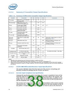
Electrical Specifications
measuring the eye diagram. The eye diagram is created using all edges of the RX test
pattern. The eye diagrams shall be measured by observing a continuous pattern at the
pin of the device. Note that the persistent eye diagram is used for determining
conformance to voltage level specifications only.
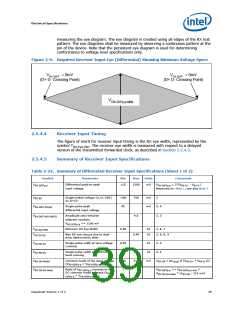
Figure 2-9. Required Receiver Input Eye (Differential) Showing Minimum Voltage Specs
VRX-DIFF = 0mV
VRX-DIFF = 0mV
(D+ D- Crossing Point)
(D+ D- Crossing Point)
VRX-DIFp-p-MIN
2.5.4.4
2.5.4.5
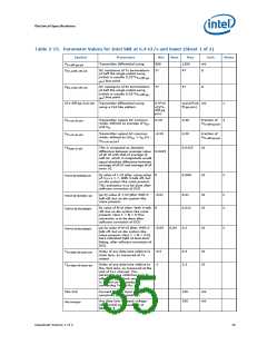
Receiver Input Timing
The figure of merit for receiver input timing is the RX eye width, represented by the
symbol TRX-Eye-Min. The receiver eye width is measured with respect to a delayed
version of the transmitted forwarded clock, as described in Section 2.5.4.5.
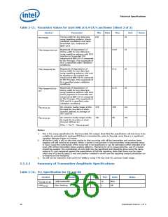
Summary of Receiver Input Specifications
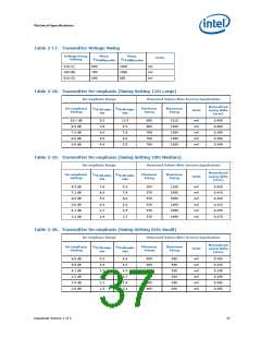
Table 2-22. Summary of Differential Receiver Input Specifications (Sheet 1 of 2)
Symbol
Parameter
Min
Max
Units
Comments
= 2*|V - V
V
Differential peak-to-peak
input voltage
115
1200
mV
V
|
RX-D-
RX-DIFFp-p
RX-DIFFp-p
RX-D+
Measured as: Note 1; see also Note 2
V
V
Single-ended voltage (w.r.t. VSS)
on D+/D-
-200
85
750
4.0
mV
mV
3
RX-SE
Single-pulse peak
differential input voltage
3, 4
RX-DIFF-PULSE
V
Amplitude ratio between
adjacent symbols,
3, 5
RX-DIFF-ADJ-RATIO
V
<= 1100 mV
RX-DIFFp-p
T
T
Minimum RX Eye Width
0.50
UI
UI
3, 6, 7
RX-Eye-MIN
RX-DJ-DD
Max RX eye closure due to dual-
dirac deterministic jitter
0.40
310
3, 6, 8, 9
T
T
Single-pulse width at zero-voltage
crossing
0.55
0.2
120
1
UI
UI
3, 4
3, 4
RX-PW-ZC
RX-PW-ML
Single-pulse width at minimum-
level crossing
V
V
Common mode of the input voltage
mV
V
= DC
of |V
+ V
|/2
RX-D-
RX-CM-MinEH
RX-CM
(avg)
RX-D+
(V
= V
)
RX-DIFFp-p
RX-DIFFp-p-min
Ratio of V
increase to max
V
V
>= V
+
RX-DIFFp-p-min
RX-CM-EH-Ratio
RX-DIFFp-p
RX-DIFFp-p
DC common mode increase (V
RX-
* (V
- 310 mV)
RX-CM
RX-CM-EH-Ratio
> V
)
DIFFp-p
RX-DIFFp-p-min
Datasheet Volume 1 of 2
39

 INTEL [ INTEL ]