Electrical Specifications
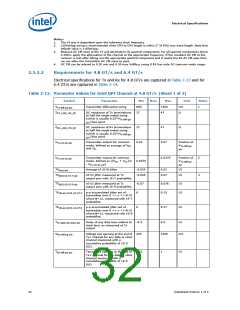
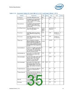
Table 2-15. Parameter Values for Intel SMI at 6.4 GT/s and lower (Sheet 1 of 2)
Symbol
Parameter
Min
800
Nom
Max
1200
Unit
Notes
V
Z
Transmitter differential swing
mV
Tx-diff-pp-pin
DC resistance of Tx terminations
at half the single ended swing
37
47
Ω
TX_LOW_CM_DC
RX_LOW_CM_DC
(which is usually 0.25*V
Tx-diff-pp-
) bias point
pin
Z
DC resistance of Rx terminations
at half the single ended swing
37
47
Ω
(which is usually 0.25*V
pin
Tx-diff-pp-
) bias point
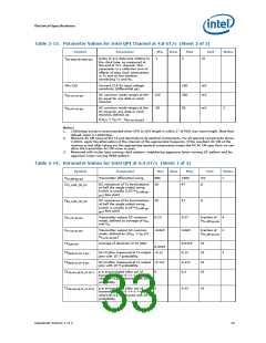
VTx-diff-pp-CLK-pin Transmitter differential swing
using a CLK like pattern
0.9*mi
n(VTx-
diff-pp
pin)
max(VTxdi mV
ff-pp-pin)
1
V
Transmitter output DC common
mode, defined as average of V
0.20
-0.20
-
0.30
Fraction of
Tx-diff-pp-pin
3
Tx-cm-dc-pin
Tx-cm-ac-pin
V
D+
and V
D-
V
Transmitter output AC common
mode, defined as ((V + V )/2 -
0.20
Fraction of
V
D+
D-
Tx-diff-pp-pin
V
)
Tx-cm-dc-pin
TX
This is computed as absolute
0.0325
UI
UI
duty-UI-pin
difference between average value 0.0325
of all UI with that of average of
odd UI, which in magnitude would
equal absolute difference between
average of all UI and average of all
even UI.
Rj value of 1-UI jitter, using setup
of Figure 2-7. With X-talk off, but
on-die system like noise present.
This extraction is to be done after
software correction of DCD
0
0.008
2
TX1UI-Rj-NoXtalk-pin
pp Dj value of 1-UI jitter With X-
talk off, but on-die system like
noise present.
-0.01
0
0.01
UI
UI
2
2
TX1UI-Dj-NoXtalk--pin
TXN-UI-Rj-NoXtalkpin
Rj value of N-UI jitter. With X-talk
off, but on-die system like noise
present. Here 1 < N < 9.This
extraction is to be done after
software correction of DCD
0.012
pp Dj value of N-UI jitter. With X- -0.04
talk off, but on-die system like
noise present. Here 1 < N < 9.Dj
here indicated Djdd of dual-dirac
fitting, after software correction of
DCD
0.04
0.2
UI
2
TXN-UI-Dj-NoXtalkpin
T
T
Delay of any data lane relative to
clock lane, as measured at Tx
output
-0.5
0.5
3.5
UI
UI
Tx-data-clk-skew-pin
Delay of any data lane relative to
the clock lane, as measured at the
end of Tx+ channel. This
-1
Rx-data-clk-skew-pin
parameter is a collective sum of
effects of data clock mismatches
in Tx and on the medium
connecting Tx and Rx.
VRx-CLK
Forward CLK Rx input voltage
sensitivity (differential pp)
150
100
mV
mV
Any data lane Rx input voltage
(differential pp) measured at
BER=1E-9
VRx-Vmargin
Datasheet Volume 1 of 2
35

 INTEL [ INTEL ]