Electrical Specifications
Notes:
1.
2.
The UI size is dependent upon the reference clock frequency
1300mVpp swing is recommended when CPU to CPU length is within 2” of PDG max trace length. Note that
default value is 1100mVpp.
3.
Measure AC CM noise at the TX and decimate to its spectral components. For all spectral components above
3.2GHz, apply the attenuation of the channel at the appropriate frequency. If the resultant AC CM at the
receiver is met after taking out the appropriate spectral component and it meets the RX AC CM spec then
we can allow the transmitter AC CM noise to pass.
4.
DC CM can be relaxed to 0.20 min and 0.30 max Vdiffp-p swing if RX has wide DC common mode range.
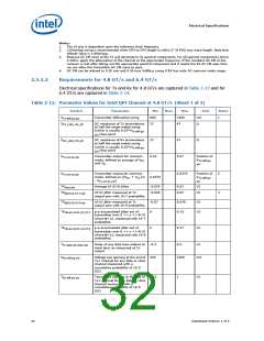
2.5.2.2
Requirements for 4.8 GT/s and 6.4 GT/s
Electrical specifications for Tx and Rx for 4.8 GT/s are captured in Table 2-13 and for
6.4 GT/s are captured in Table 2-14.
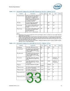
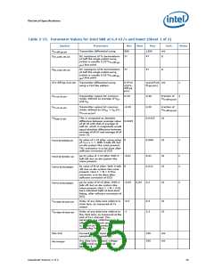
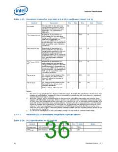
Table 2-13. Parameter Values for Intel QPI Channel at 4.8 GT/s (Sheet 1 of 2)
Symbol
Parameter
Min
800
Nom
Max
1500
Unit
Notes
V
Z
Transmitter differential swing
mV
1
Tx-diff-pp-pin
DC resistance of Tx terminations
at half the single ended swing
37
47
Ω
TX_LOW_CM_DC
(which is usually 0.25*V
Tx-diff-pp-
) bias point
pin
Z
V
DC resistance of Rx terminations
at half the single ended swing
37
47
Ω
RX_LOW_CM_DC
Tx-cm-dc-pin
(which is usually 0.25*V
pin
Tx-diff-pp-
) bias point
Transmitter output DC common
mode, defined as average of V
0.23
0.27
Fraction of
V
D+
Tx-diff-pp-
and V
D-
pin
V
Transmitter output AC common
mode, defined as ((V + V )/2
-
0.0375
Fraction of
Tx-diff-pp-
pin
UI
2
3
Tx-cm-ac-pin
0.0375
V
D+
D-
- V
)
Tx-cm-dc-pin
TX
TX
Average of UI-UI jitter.
-0.025
-0.065
0.03
0.07
duty-pin
UI-UI jitter measured at Tx
output pins with 1E-7 probability.
UI
UI
UI
jitUI-UI-1E-7-pin
TX
TX
UI-UI jitter measured at Tx
output pins with 1E-9 probability.
-0.07
0
0.076
0.15
jitUI-UI-1E-9-pin
p-p accumulated jitter out of
transmitter over 0 <= n <= N UI
where N=12, measured with 1E-7
probability.
clk-acc-jit-N_UI-1E-7
TX
p-p accumulated jitter out of
transmitter over 0 <= n <= N UI
where N=12, measured with 1E-9
probability.
0
0.17
UI
clk-acc-jit-N_UI-1E-9
Tx-data-clk-skew-pin
T
Delay of any data lane relative to
clock lane, as measured at Tx
output
-0.5
0.5
UI
V
Voltage eye opening at the end of 225
Tx+ channel for any data or clock
channel measured with a
cumulative probability of 1E-9
(UI).
1200
mV
Rx-diff-pp-pin
T
Timing eye opening at the end of
Tx+ channel for any data or clock
channel measured with a
cumulative probability of 1E-9
(UI)
0.63
1
UI
Rx-diff-pp-pin
32
Datasheet Volume 1 of 2

 INTEL [ INTEL ]