Electrical Specifications
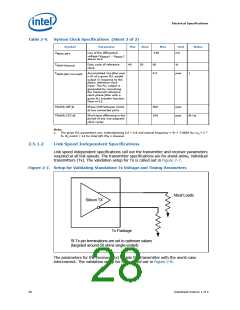
Table 2-9.
System Clock Specifications (Sheet 2 of 2)
Symbol
Parameter
Min
Nom
Max
Unit
mV
Notes
V
Low of the differential
-150
Refclk_diff-il
voltage (V
+ - V
-)
Refclk
Refclk
above zero
T
T
Duty cycle of reference
clock.
40
50
60
%
Refclk-Dutycycle
Accumulated rms jitter over
n UI of a given PLL model
output in response to the
jittery reference clock
input. The PLL output is
generated by convolving
the measured reference
clock phase jitter with a
given PLL transfer function.
Here n=12.
0.5
psec
1
Refclk-jitter-rms-onepll
TRefclk-diff-jit
TRefclk-C2C-jit
Phase Drift between clocks
at two connected ports
500
100
psec
psec
Short term difference in the
period of any two adjacent
clock cycles
At via
Note:
1.
The given PLL parameters are: Underdamping (z) = 0.8 and natural frequency = fn = 7.86E6 Hz; w = 2 *
n
fn. N_minUI = 12 for Intel QPI Phy 1 channel.
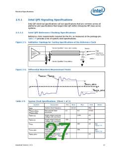
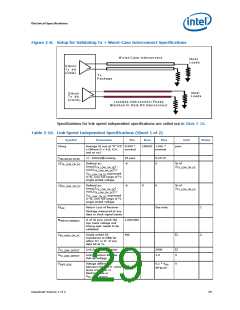
2.5.1.2
Link Speed Independent Specifications
Link speed independent specifications call out the transmitter and receiver parameters
required at all link speeds. The transmitter specifications are for stand-alone, individual
transmitters (Tx). The validation setup for Tx is called out in Figure 2-7.
Figure 2-7. Setup for Validating Standalone Tx Voltage and Timing Parameters
Ideal Loads
Silicon TX
Tx Package
SI Tx pin terminations are set to optimum values
(targeted around 50 ohms single-ended)
The parameters for the receiver (Rx) couple the transmitter with the worst-case
interconnect. The validation setup for Rx is called out in Figure 2-8.
28
Datasheet Volume 1 of 2

 INTEL [ INTEL ]