Electrical Specifications
Notes:
1. This speed is the 1/4 RefClk Frequency.
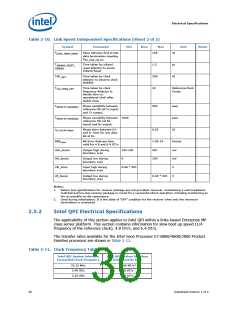
2.5.2.1
Requirements at 1/4 RefClk Signaling Rate
The signaling rate is defined as 1/4 the rate of the System Reference Clock. For
example, a 133 MHz System Reference Clock would have a forwarded clock frequency
of 33.33 MHz and the signaling rate would be 66.66 MT/s.
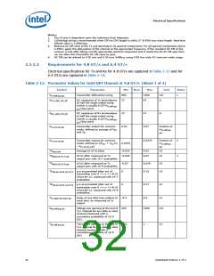
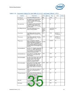
Table 2-12. Parameter Values for Intel® QPI Phy1 Channel at 1/4 RefClk Frequency
Symbol
Parameter
Min
Nom
Max
Unit
Notes
mV
1
V
Z
Transmitter differential swing
800
1500
Tx-diff-pp-pin
Ω
DC resistance of Tx terminations
at half the single ended swing
37
47
TX_LOW_CM_DC
(which is usually 0.25*V
pin
Tx-diff-pp-
) bias point
Ω
DC resistance of Rx terminations
at half the single ended swing
Z
37
47
RX_LOW_CM_DC
(which is usually 0.25*V
Tx-diff-pp-
) bias point
pin
5
2
Transmitter output DC common
mode, defined as average of V
Fraction of
V
V
0.23
0.27
V
Tx-cm-dc-pin
D+
Tx-diff-pp-pin
and V
D-
Transmitter output AC common
mode, defined as ((V + V )/2 -
Fraction of
-
0.0375
0.0025
0.0075
V
Tx-cm-ac-pin
D+
D-
Tx-diff-pp-pin
0.0375
V
)
Tx-cm-dc-pin
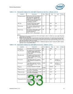
UI
UI
1
3
TX
TX
Average of absolute UI-UI jitter
-0.002
-0.007
duty-pin
Absolute value of UI-UI jitter
measured at Tx output pins with
1E-7 probability.
jitUI-UI-1E-7-pin
mV
Voltage eye opening at the end of
Tx+ channel for any data or clock
channel measured with a
cumulative probability of 1E-9
(UI).
V
150
0.9
V
1
Rx-diff-pp-pin
Tx-diff-pp-pin
T
Timing eye opening at the end of
Tx+ channel for any data or clock
channel measured with a
cumulative probability of 1E-9
(UI).
UI
UI
Rx-diff-pp-pin
T
Delay of any data lane relative to
the clock lane, as measured at the
end of Tx+ channel. This
0.48
0.52
Rx-data-clk-skew-pin
parameter is a collective sum of
effects of data clock mismatches
in Tx and on the medium
connecting Tx and Rx.
VRx-CLK
Forward CLK Rx input voltage
sensitivity (differential pp)
150
400
mV
mV
V
DC common mode ranges at the
Rx input for any data or clock
channel
75
Rx-cm-dc-pin
Rx-cm-ac-pin
V
AC common mode ranges at the
Rx input for any data or clock
channel, defined as:
-50
50
mV
2
((V
+ V /2 - V
)
RX-cm-dc-pin
D+
D-
Datasheet Volume 1 of 2
31

 INTEL [ INTEL ]