Electrical Specifications
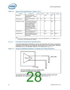
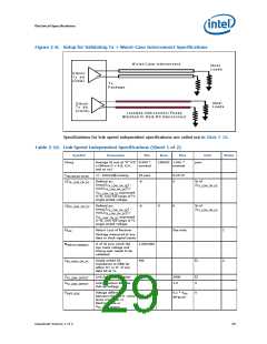
Figure 2-8. Setup for Validating Tx + Worst-Case Interconnect Specifications
W o rs t-C a s e In te rc o n n e c t
Id e a l
L o a d s
S ilic o n
T x b it
(D a ta )
T x
P a c k a g e
Id e a l
L o a d s
S ilic o n
T x b it
(C lo c k )
L o s s le s s In te rc o n n e c t P h a s e
M a tc h e d to D a ta B it In te rc o n n e c t
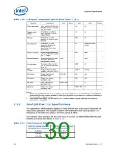
Specifications for link speed independent specifications are called out in Table 2-10.
Table 2-10. Link Speed Independent Specifications (Sheet 1 of 2)
Symbol
UIavg
Parameter
Min
Nom
Max
Unit
Notes
Average UI size at “G” GT/ 0.999 *
s (Where G = 4.8, 6.4,
and so on)
1000/G 1.001 *
nominal
psec
% of
nominal
T
+/- 100mV@crossing
25 psec
-6
0.25 UI
6
rise-fall-pin-20-80
ΔZ
ΔZ
RL
Defined as:
TX_LOW_CM_DC
(max(Z
) -
Z
TX_LOW_CM_DC
TX_LOW_CM_DC
min(Z
Z
)) /
TX_LOW_CM_DC
expressed
TX_LOW_CM_DC
in %, over full range of Tx
single ended voltage
Defined as:
-6
0
6
% of
Z
RX_LOW_CM_DC
(max(Z
) -
)) /
TX_LOW_CM_DC
TX_LOW_CM_DC
min(Z
Z
TX_LOW_CM_DC
expressed
TX_LOW_CM_DC
in %, over full range of Tx
single ended voltage
Return Loss of Receiver
See note
1
RX
Package measured at any
data or clock signal inputs
N
Z
# of UI over which the
eye mask voltage and
timing spec needs to be
validated
1,000,000
40k
MIN-UI-Validation
Single ended DC
Ω
2
RX_HIGH_CM_DC
impedance to GND for
either D+ or D- of any
data bit at Tx
Z
V
Link Detection Resistor
500
2000
1.5
Ω
TX_LINK_DETECT
Link Detection Resistor
Pull-up Voltage
V
TX_LINK_DETECT
V
Voltage difference
between D+ and D- when
lanes are either in
Electrical Idle or
0.1 * V
V
DIFF_IDLE
Rx-
diff-pp-pin
V
TX_LINK_DETECT
Datasheet Volume 1 of 2
29

 INTEL [ INTEL ]