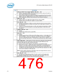
LPC Interface Bridge Registers (D31:F0)
Bit
Description
Software SMI# Timer Enable (SWSMI_TMR_EN) — R/W.
0 = Disable. Clearing the SWSMI_TMR_EN bit before the timer expires will reset the
timer and the SMI# will not be generated.
1 = Starts Software SMI# Timer. When the SWSMI timer expires (the timeout period
depends upon the SWSMI_RATE_SEL bit setting), SWSMI_TMR_STS is set and an
SMI# is generated. SWSMI_TMR_EN stays set until cleared by software.
6
APMC_EN — R/W.
5
4
3
2
0 = Disable. Writes to the APM_CNT register will not cause an SMI#.
1 = Enables writes to the APM_CNT register to cause an SMI#.
SLP_SMI_EN — R/W.
0 = Disables the generation of SMI# on SLP_EN. Note that this bit must be 0 before
the software attempts to transition the system into a sleep state by writing a 1 to
the SLP_EN bit.
1 = A write of 1 to the SLP_EN bit (bit 13 in PM1_CNT register) will generate an SMI#,
and the system will not transition to the sleep state based on that write to the
SLP_EN bit.
LEGACY_USB_EN — R/W.
0 = Disable.
1 = Enables legacy USB circuit to cause SMI#.
BIOS_EN — R/W.
0 = Disable.
1 = Enables the generation of SMI# when ACPI software writes a 1 to the GBL_RLS bit
(D31:F0:PMBase + 04h:bit 2). Note that if the BIOS_STS bit (D31:F0:PMBase +
34h:bit 2), which gets set when software writes 1 to GBL_RLS bit, is already a 1 at
the time that BIOS_EN becomes 1, an SMI# will be generated when BIOS_EN gets
set.
End of SMI (EOS) — R/W (special). This bit controls the arbitration of the SMI signal
to the processor. This bit must be set for the ICH10 to assert SMI# low to the
processor after SMI# has been asserted previously.
0 = Once the ICH10 asserts SMI# low, the EOS bit is automatically cleared.
1 = When this bit is set to 1, SMI# signal will be deasserted for 4 PCI clocks before its
assertion. In the SMI handler, the processor should clear all pending SMIs (by
servicing them and then clearing their respective status bits), set the EOS bit, and
exit SMM. This will allow the SMI arbiter to re-assert SMI upon detection of an SMI
event and the setting of a SMI status bit.
1
0
NOTE: ICH10 is able to generate 1st SMI after reset even though EOS bit is not set.
Subsequent SMI require EOS bit is set.
GBL_SMI_EN — R/W.
0 = No SMI# will be generated by ICH10. This bit is reset by a PCI reset event.
1 = Enables the generation of SMI# in the system upon any enabled SMI event.
NOTE: When the SMI_LOCK bit is set, this bit cannot be changed.
476
Datasheet

 INTEL [ INTEL ]