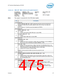
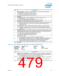
LPC Interface Bridge Registers (D31:F0)
Bit
Description
PM1_STS_REG — RO. This is an ORs of the bits in the ACPI PM1 Status Register
(offset PMBASE+00h) that can cause an SMI#.
8
0 = SMI# was not generated by a PM1_STS event.
1 = SMI# was generated by a PM1_STS event.
7
6
Reserved
SWSMI_TMR_STS — R/WC. Software clears this bit by writing a 1 to it.
0 = Software SMI# Timer has Not expired.
1 = Set by the hardware when the Software SMI# Timer expires.
APM_STS — R/WC. Software clears this bit by writing a 1 to it.
0 = No SMI# generated by write access to APM Control register with APMCH_EN bit set.
1 = SMI# was generated by a write access to the APM Control register with the
APMC_EN bit set.
5
4
SLP_SMI_STS — R/WC. Software clears this bit by writing a 1 to the bit location.
0 = No SMI# caused by write of 1 to SLP_EN bit when SLP_SMI_EN bit is also set.
1 = Indicates an SMI# was caused by a write of 1 to SLP_EN bit when SLP_SMI_EN bit
is also set.
LEGACY_USB_STS — RO. This bit is a logical OR of each of the SMI status bits in the
USB Legacy Keyboard/Mouse Control Registers ANDed with the corresponding enable
bits. This bit will not be active if the enable bits are not set.
3
0 = SMI# was not generated by USB Legacy event.
1 = SMI# was generated by USB Legacy event.
BIOS_STS — R/WC.
0 = No SMI# generated due to ACPI software requesting attention.
1 = This bit gets set by hardware when a 1 is written by software to the GBL_RLS bit
(D31:F0:PMBase + 04h:bit 2). When both the BIOS_EN bit (D31:F0:PMBase +
30h:bit 2) and the BIOS_STS bit are set, an SMI# will be generated. The
BIOS_STS bit is cleared when software writes a 1 to its bit position.
2
1:0
Reserved
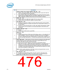
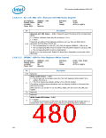
13.8.3.13 ALT_GP_SMI_EN—Alternate GPI SMI Enable Register
I/O Address:
Default Value:
Lockable:
PMBASE +38h
0000h
Attribute:
Size:
Usage:
R/W
16-bit
No
ACPI or Legacy
Power Well:
Resume
Bit
Description
Alternate GPI SMI Enable — R/W. These bits are used to enable the corresponding
GPIO to cause an SMI#. For these bits to have any effect, the following must be true.
• The corresponding bit in the ALT_GP_SMI_EN register is set.
15:0
• The corresponding GPI must be routed in the GPI_ROUT register to cause an SMI.
• The corresponding GPIO must be implemented.
NOTE: Mapping is as follows: bit 15 corresponds to GPIO15... bit 0 corresponds to
GPIO0.
Datasheet
479

 INTEL [ INTEL ]