LPC Interface Bridge Registers (D31:F0)
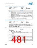
13.8.3.14 ALT_GP_SMI_STS—Alternate GPI SMI Status Register
I/O Address:
Default Value:
Lockable:
PMBASE +3Ah
0000h
Attribute:
Size:
Usage:
R/WC
16-bit
No
ACPI or Legacy
Power Well:
Resume
Bit
Description
Alternate GPI SMI Status — R/WC. These bits report the status of the corresponding
GPIOs.
0 = Inactive. Software clears this bit by writing a 1 to it.
1 = Active
These bits are sticky. If the following conditions are true, then an SMI# will be
generated and the GPE0_STS bit set:
15:0
• The corresponding bit in the ALT_GPI_SMI_EN register (PMBASE + 38h) is set
• The corresponding GPIO must be routed in the GPI_ROUT register to cause an SMI.
• The corresponding GPIO must be implemented.
All bits are in the resume well. Default for these bits is dependent on the state of the
GPIO pins.
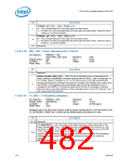
13.8.3.15 UPRWC—USB Per-Port Registers Write Control
I/O Address:
Default Value:
Lockable:
PMBASE +3Ch
0000h
Attribute:
Size:
Usage:
R/WC, R/W, R/WO
16-bit
ACPI or Legacy
No
Power Well:
Resume
Bit
Description
15:9 Reserved
Write Enable Status — R/WC
0 = This bit gets set by hardware when the “Per-Port Registers Write Enable” bit is
written from 0-to-1.
1 = This bit is cleared by software writing a 1b to this bit location
8
The setting condition takes precedence over the clearing condition in the event that
both occur at once.
When this bit is 1b and bit 0 is 1b, the INTEL_USB2_STS bit is set in the SMI_STS
register.
7:2
1
Reserved.
Reserved
Write Enable SMI Enable— R/WO
0 = Disable
0
1 = enables the generation of SMI when the Per-Port Registers Write Enable (bit 1) is
written from 0 to 1. Once written to 1b, this bit can not be cleared by software.
480
Datasheet

 INTEL [ INTEL ]