LPC Interface Bridge Registers (D31:F0)
13.8.1.8
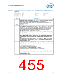
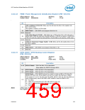
PMIR—Power Management Initialization Register (PM—D31:F0)
Offset Address: ACh
Attribute:
Size:
R/W
32-bit
Default Value:
00000000h
0
Bit
Description
CF9h Lockdown (CF9LOCK): When set, this bit locks the bits in this register into
their current value.
31
30
This register is reset by a CF9h reset.
PMIR Field 2 — R/W. BIOS must program this bit to 1b.
29:21 Reserved
CF9h Global Reset (CF9GR)— R/W. When set, a CF9h write of 6h or Eh will cause a
20
Global reset of both the Host and Intel ME partitions. If this bit is cleared, a CF9h write
of 6h or Eh will only reset the host partition. This bit field is not reset by a CF9h reset.
19:15 Reserved
Intel® AT Host Reset Trigger Enable - R/W. When set this bit enables bits [1:0] in
the CIR11 register.
13:10 Reserved
14
9:8
7:0
PMIR Field 0 — R/W. BIOS must program these bits to 11b.
Reserved
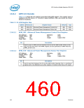
13.8.1.9
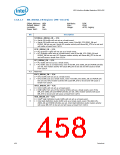
GPIO_ROUT—GPIO Routing Control Register
(PM—D31:F0)
Offset Address: B8h – BBh
Attribute:
Size:
Power Well:
R/W
32-bit
Resume
Default Value:
Lockable:
00000000h
No
Bit
Description
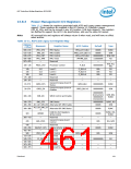
31:30 GPIO15 Route — R/W. See bits 1:0 for description.
Same pattern for GPIO14 through GPIO3
5:4
3:2
GPIO2 Route — R/W. See bits 1:0 for description.
GPIO1 Route — R/W. See bits 1:0 for description.
GPIO0 Route — R/W. GPIO[15:0] can be routed to cause an SMI or SCI when the
GPIO[n]_STS bit is set. If the GPIO0 is not set to an input, this field has no effect.
If the system is in an S1–S5 state and if the GPE0_EN bit is also set, then the GPIO can
cause a Wake event, even if the GPIO is NOT routed to cause an SMI# or SCI.
1:0
00 = No effect.
01 = SMI# (if corresponding ALT_GPI_SMI_EN bit is also set)
10 = SCI (if corresponding GPE0_EN bit is also set)
11 = Reserved
Note:
GPIOs that are not implemented will not have the corresponding bits implemented in
this register.
Datasheet
459

 INTEL [ INTEL ]