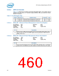
LPC Interface Bridge Registers (D31:F0)
13.8.3
Power Management I/O Registers
Table 13-11 shows the registers associated with ACPI and Legacy power management
support. These registers are enabled in the PCI Device 31: Function 0 space
(PM_IO_EN), and can be moved to any I/O location (128-byte aligned). The registers
are defined to support the ACPI 3.0a specification, and use the same bit names.
Note:
All reserved bits and registers will always return 0 when read, and will have no effect
when written.
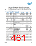
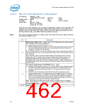
Table 13-11. ACPI and Legacy I/O Register Map
PMBASE
Mnemonic
Register Name
ACPI Pointer
Default
Type
+ Offset
00h–01h
02h–03h
04h–07h
08h–0Bh
0Ch–0Fh
PM1_STS
PM1_EN
PM1_CNT
PM1_TMR
—
PM1 Status
PM1a_EVT_BLK
PM1a_EVT_BLK+2
PM1a_CNT_BLK
PMTMR_BLK
—
0000h
0000h
R/WC
R/W
PM1 Enable
PM1 Control
PM1 Timer
Reserved
00000000h
xx000000h
—
R/W, WO
RO
—
R/W, RO,
WO
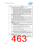
10h–13h
PROC_CNT
Processor Control
P_BLK
00000000h
14h
15h
LV2
LV3
LV4
—
Level 2
P_BLK+4
P_BLK+5
P_BLK+6
—
00h
00h
00h
—
RO
RO
RO
—
Level 3
16h
Level 4
17h–18h
19h–1Fh
Reserved
Reserved
—
—
—
—
General Purpose Event 0
Status
20-27h
28-2Fh
GPE0_STS
GPE0_EN
GPE0_BLK
00000000h
00000000h
R/WC
R/W
General Purpose Event 0
Enables
GPE0_BLK+8
00000000h
(Consumer);
00000002h
(Corporate)
R/W, WO,
R/WO
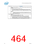
30h–33h
34h–37h
SMI_EN
SMI# Control and Enable
SMI Status
SMI_STS
00000000h
0000h
R/WC, RO
R/W
38h–39h ALT_GP_SMI_EN Alternate GPI SMI Enable
ALT_GP_SMI_ST
3Ah–3Bh
Alternate GPI SMI Status
0000h
R/WC
S
UPRWC
—
USB Per-Port Registers
Write Control
R/WC, RO,
R/WO
3Ch
3Dh–41h
42h
0000h
—
Reserved
—
—
—
General Purpose Event
Control
GPE_CNTL
00h
RO, R/W
43h
—
Reserved
—
—
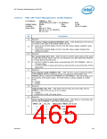
44h–45h
46h–4Fh
50h
DEVACT_STS
Device Activity Status
Reserved
0000h
R/WC
—
PM2_CNT
PM2 Control
PM2a_CNT_BLK
—
00h
R/W
RO
51h-53h
54h–57h
58h-5Bh
5Ch–5Fh
60h–7Fh
—
C3_RES
—
Reserved
C3-Residency Register
Reserved
00000000h
—
Reserved
—
—
—
—
—
—
—
Reserved for TCO
Datasheet
461

 INTEL [ INTEL ]