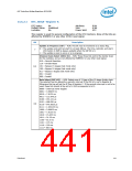
LPC Interface Bridge Registers (D31:F0)
Bit
Description
Speaker Data Enable (SPKR_DAT_EN) — R/W.
1
0
0 = SPKR output is a 0.
1 = SPKR output is equivalent to the Counter 2 OUT signal value.
Timer Counter 2 Enable (TIM_CNT2_EN) — R/W.
0 = Disable
1 = Enable
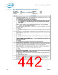
13.7.2
NMI_EN—NMI Enable (and Real Time Clock Index)
Register (LPC I/F—D31:F0)
I/O Address:
Default Value:
Lockable:
70h
80h
No
Attribute:
Size:
Power Well:
R/W (special)
8-bit
Core
Note:
The RTC Index field is write-only for normal operation. This field can only be read in Alt-
Access Mode. Note, however, that this register is aliased to Port 74h (documented in),
and all bits are readable at that address.
Bits
Description
NMI Enable (NMI_EN) — R/W (special).
7
0 = Enable NMI sources.
1 = Disable All NMI sources.
Real Time Clock Index Address (RTC_INDX) — R/W (special). This data goes to
the RTC to select which register or CMOS RAM address is being accessed.
6:0
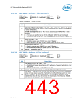
13.7.3
PORT92—Fast A20 and Init Register (LPC I/F—D31:F0)
I/O Address:
Default Value:
Lockable:
92h
00h
No
Attribute:
Size:
Power Well:
R/W
8-bit
Core
Bit
Description
7:2
Reserved
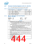
Alternate A20 Gate (ALT_A20_GATE) — R/W. This bit is Or’d with the A20GATE
input signal to generate A20M# to the processor.
1
0 = A20M# signal can potentially go active.
1 = This bit is set when INIT# goes active.
INIT_NOW — R/W. When this bit transitions from a 0 to a 1, the ICH10 will force
INIT# active for 16 PCI clocks.
0
Datasheet
445

 INTEL [ INTEL ]