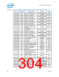
Chipset Configuration Registers
Table 10-1. Chipset Configuration Register Memory Map (Memory Space) (Sheet 2 of 4)
Offset
Mnemonic
Register Name
Default
Type
0118–011Fh
0120–0123h
0128–012Fh
0130–0133h
0138–013Fh
0140–0143h
0148–014Fh
0150–0153h
0158–015Fh
ULBA
RP1D
Upstream Link Base Address
Root Port 1 Descriptor
Root Port 1 Base Address
Root Port 2 Descriptor
Root Port 2 Base Address
Root Port 3 Descriptor
Root Port 3 Base Address
Root Port 4 Descriptor
Root Port 4 Base Address
0000000000000000h
01xx0002h
R/WO
R/WO, RO
RO
RP1BA
RP2D
00000000000E0000h
02xx0002h
R/WO, RO
RO
RP2BA
RP3D
00000000000E1000h
03xx0002h
R/WO, RO
RO
RP3BA
RP4D
00000000000E2000h
04xx0002h
R/WO, RO
RO
RP4BA
00000000000E3000h
Intel® High Definition Audio
Descriptor
0160–0163h
0168–016Fh
HDD
15xx0002h
R/WO, RO
RO
Intel High Definition Audio
Base Address
HDBA
00000000000D8000h
0170–0173h
0178–017Fh
0180–0183h
0188–018Fh
01A0–01A3h
01A4–01A7h
01A8–01A9h
01AA–01ABh
01F4-01F7h
01FC-01FDh
0220-0223h
0224–0227h
0234-0327h
RP5D
RP5A
RP6D
RP6BA
ILCL
Root Port 5 Descriptor
Root Port 5 Base Address
Root Port 6 Descriptor
Root Port 6 Base Address
Internal Link Capability List
Link Capabilities
05xx0002h
00000000000E4000h
06xx0002h
00000000000E5000h
00010006h
00012841h
0000h
R/WO, RO
RO
R/WO, RO
RO
RO
LCAP
LCTL
LSTS
CIR2
CIR3
BCR
RO, R/WO
R/W
Link Control
Link Status
0041h
RO
Chipset Initialization Register 2
Chipset Initialization Register 3
Backbone Configuration
Root Port Configuration
DMI Control
00000000h
0000h
R/W
R/W
00000000h
0000000yh
00000000h
R/W
RPC
R/W, RO
R/W, RO
DMIC
Root Port Function Number for
PCI Express Root Ports
0238–023Bh
0290-0293h
0F20-0F23h
RPFN
FPSS
00543210h
00000000h
B2B477CCh
R/WO, RO
RO
Function Level Reset Pending
Status Summary
Chipset Initialization Register
13
CIR13
R/W
1D40-1D47h
1E00–1E03h
1E10–1E17h
1E18-1E1Fh
1E80-1E87h
1E88-1E8Fh
1E90-1E97h
CIR5
TRSR
TRCR
TWDR
IOTR0
IOTR1
IOTR2
Chipset Initialization Register 5 0000000000000000h
R/W
R/WC, RO
RO
Trap Status Register
Trapped Cycle Register
Trapped Write Data Register
I/O Trap Register 0
00000000h
0000000000000000h
0000000000000000h
0000000000000000h
0000000000000000h
0000000000000000h
RO
R/W
I/O Trap Register 1
R/W
I/O Trap Register 2
R/W
304
Datasheet

 INTEL [ INTEL ]