Chipset Configuration Registers
10 Chipset Configuration Registers
This section describes all registers and base functionality that is related to chipset
configuration and not a specific interface (such as LPC, PCI, or PCI Express*). It
contains the root complex register block, which describes the behavior of the upstream
internal link.
This block is mapped into memory space, using the Root Complex Base Address (RCBA)
register of the PCI-to-LPC bridge. Accesses in this space must be limited to 32-(DW) bit
quantities. Burst accesses are not allowed.
All Chipset Configuration Registers are located in the core well unless otherwise
indicated.
10.1
Chipset Configuration Registers (Memory Space)
Note:
Address locations that are not shown should be treated as Reserved (see Section 9.2
for details).
.
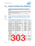
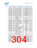
Table 10-1. Chipset Configuration Register Memory Map (Memory Space) (Sheet 1 of 4)
Offset
Mnemonic
Register Name
Default
Type
Virtual Channel Capability
Header
0000–0003h
VCH
10010002h
R/WO
0004–0007h
0008–000Bh
000C–000Dh
000E–000Fh
0010–0013h
0014–0017h
001A–001Bh
001C–001Fh
0020–0023h
0026–0027h
VCAP1
VCAP2
PVC
Virtual Channel Capability #1
Virtual Channel Capability #2
Port VC Control
00000801h
00000001h
0000h
RO, R/WO
RO
RO, R/W
RO
PVS
Port VC Status
0000h
V0CAP
V0CTL
V0STS
V1CAP
V1CTL
V1STS
VC 0 Resource Capability
VC 0 Resource Control
VC 0 Resource Status
VC 1 Resource Capability
VC 1 Resource Control
VC 1 Resource Status
00000001h
800000FFh
0000h
RO
R/W, RO
RO
03008011h
00000000h
0000h
R/WO, RO
R/W
RO
0030-006Fh
(Corporate
Only)
—
Reserved
—
—
0030-006Fh
(Consumer
Only)
PAT
Port Arbitration Table
0088-008Bh
00AC-00AFh
CIR1
REC
Chipset Initialization Register 1
Root Error Command
00000000h
0000h
R/WO
R/W
Root Complex Topology
Capability List
0100–0103h
RCTCL
1A010005h
RO
0104–0107h
0110–0113h
ESD
ULD
Element Self Description
Upstream Link Descriptor
00000802h
00000001h
R/WO, RO
R/WO, RO
Datasheet
303

 INTEL [ INTEL ]