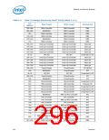
Register and Memory Mapping
Table 9-4.
Memory Decode Ranges from Processor Perspective (Sheet 2 of 2)
Memory Range
Target
Dependency/Comments
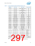
FFE0 000h–FFE7 FFFFh
FFA0 0000h–FFA7 FFFFh
Firmware Hub (or
PCI)2
Bit 12 in Firmware Hub Decode Enable register
is set
FFE8 0000h–FFEF FFFFh
FFA8 0000h–FFAF FFFFh
Firmware Hub (or
PCI)3
Bit 13 in Firmware Hub Decode Enable register
is set
FFF0 0000h–FFF7 FFFFh
FFB0 0000h–FFB7 FFFFh
Firmware Hub (or
PCI)2
Bit 14 in Firmware Hub Decode Enable register
is set
Always enabled.
The top two, 64 KB blocks of this range can be
swapped, as described in Section 7.4.1.
FFF8 0000h–FFFF FFFFh
FFB8 0000h–FFBF FFFFh
Firmware Hub (or
PCI)2
FF70 0000h–FF7F FFFFh
FF30 0000h–FF3F FFFFh
Firmware Hub (or
PCI)2
Bit 3 in Firmware Hub Decode Enable register
is set
FF60 0000h–FF6F FFFFh
FF20 0000h–FF2F FFFFh
Firmware Hub (or
PCI)2
Bit 2 in Firmware Hub Decode Enable register
is set
FF50 0000h–FF5F FFFFh
FF10 0000h–FF1F FFFFh
Firmware Hub (or
PCI)2
Bit 1 in Firmware Hub Decode Enable register
is set
FF40 0000h–FF4F FFFFh
FF00 0000h–FF0F FFFFh
Firmware Hub (or
PCI)2
Bit 0 in Firmware Hub Decode Enable register
is set
128 KB anywhere in 4-GB
range
Integrated LAN
Controller
Enable via BAR in Device 25:Function 0
(Integrated LAN Controller)
1 KB anywhere in 4-GB
range
USB EHCI
Enable via standard PCI mechanism (Device
29, Function 7)
Controller #11
1 KB anywhere in 4-GB
range
USB EHCI
Enable via standard PCI mechanism (Device
26, Function 7)
Controller #21
Intel® High
Definition Audio
Host Controller
512 B anywhere in 64-bit
addressing space
Enable via standard PCI mechanism (Device
27, Function 0)
BIOS determines the “fixed” location which is
one of four, 1-KB ranges where X (in the first
column) is 0h, 1h, 2h, or 3h.
High Precision
Event Timers 1
FED0 X000h–FED0 X3FFh
All other
PCI
None
NOTES:
1.
Software must not attempt locks to memory mapped I/O ranges for USB EHCI or High
Precision Event Timers. If attempted, the lock is not honored, which means potential
deadlock conditions may occur.
2.
PCI is the target when the Boot BIOS Destination selection bits are set to 10b (Chipset
Config Registers:Offset 3401 bits 11:10). When PCI selected, the Firmware Hub Decode
Enable bits have no effect.
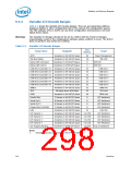
9.4.1
Boot-Block Update Scheme
The ICH10 supports a “top-block swap” mode that has the ICH10 swap the top block in
the Firmware Hub (the boot block) with another location. This allows for safe update of
the Boot Block (even if a power failure occurs). When the “TOP_SWAP” Enable bit is
set, the ICH10 will invert A16 for cycles targeting Firmware Hub space. When this bit is
0, the ICH10 will not invert A16. This bit is automatically set to 0 by RTCRST#, but not
by PLTRST#.
300
Datasheet

 INTEL [ INTEL ]