Register and Memory Mapping
9.4
Memory Map
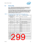
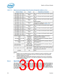
Table 9-4 shows (from the processor perspective) the memory ranges that the ICH10
decodes. Cycles that arrive from DMI that are not directed to any of the internal
memory targets that decode directly from DMI will be driven out on PCI unless the
Subtractive Decode Policy bit is set (D31:F0:Offset 42h, bit 0).
PCI cycles generated by external PCI masters will be positively decoded unless they fall
in the PCI-to-PCI bridge memory forwarding ranges (those addresses are reserved for
PCI peer-to-peer traffic). If the cycle is not in the internal LAN controller’s range, it will
be forwarded up to DMI. Software must not attempt locks to the ICH10’s memory-
mapped I/O ranges for EHCI and HPET. If attempted, the lock is not honored which
means potential deadlock conditions may occur.
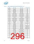
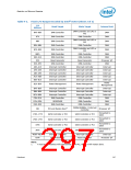
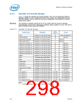
Table 9-4.
Memory Decode Ranges from Processor Perspective (Sheet 1 of 2)
Memory Range
Target
Dependency/Comments
0000 0000h–000D FFFFh
Main Memory
TOM registers in Host controller
0010 0000h–TOM
(Top of Memory)
Bit 6 in Firmware Hub Decode Enable register
is set
000E 0000h–000E FFFFh
000F 0000h–000F FFFFh
Firmware Hub
Firmware Hub
Bit 7 in Firmware Hub Decode Enable register
is set
FEC_ _000h–FEC_ _040h
(Corporate Only)
IO(x) APIC inside
ICH10
_ _is controlled via APIC Range Select (ASEL)
field and APIC Enable (AEN) bit
FEC0 _000h–FEC0 _040h
(Consumer Only)
IO(x) APIC inside
ICH10
_ is controlled via APIC Range Select (ASEL)
field and APIC Enable (AEN) bit
PCI Express* Root Port 1 I/OxAPIC Enable
(PAE) set
FEC1 0000h–FEC1 7FFF
PCI Express* Port 1
PCI Express* Root Port 2 I/OxAPIC Enable
(PAE) set
FEC1 8000h–FEC1 8FFFh PCI Express* Port 2
FEC2 0000h–FEC2 7FFFh PCI Express* Port 3
FEC2 8000h–FEC2 8FFFh PCI Express* Port 4
FEC3 0000h–FEC3 7FFFh PCI Express* Port 5
FEC3 8000h–FEC3 8FFFh PCI Express* Port 6
PCI Express* Root Port 3 I/OxAPIC Enable
(PAE) set
PCI Express* Root Port 4 I/OxAPIC Enable
(PAE) set
PCI Express* Root Port 5 I/OxAPIC Enable
(PAE) set
PCI Express* Root Port 6 I/OxAPIC Enable
(PAE) set
FED4 0000h–FED4 BFFFh
TPM on LPC
FFC0 0000h–FFC7 FFFFh
FF80 0000h–FF87 FFFFh
Firmware Hub (or
PCI)2
Bit 8 in Firmware Hub Decode Enable register
is set
FFC8 0000h–FFCF FFFFh
FF88 0000h–FF8F FFFFh
Firmware Hub (or
PCI)2
Bit 9 in Firmware Hub Decode Enable register
is set
FFD0 0000h–FFD7 FFFFh
FF90 0000h–FF97 FFFFh
Firmware Hub (or
PCI)2
Bit 10 in Firmware Hub Decode Enable register
is set
FFD8 0000h–FFDF FFFFh
FF98 0000h–FF9F FFFFh
Firmware Hub (or
PCI)2
Bit 11 in Firmware Hub Decode Enable register
is set
Datasheet
299

 INTEL [ INTEL ]