Functional Description
5.4.1.1
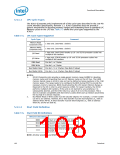
LPC Cycle Types
The ICH10 (Corporate only) implements all of the cycle types described in the Low Pin
Count Interface Specification, Revision 1.1. ICH10 Consumer does not provide a
generic mechanism for decoding memory ranges and forwarding them as standard LPC
Memory cycles on the LPC bus. Table 5-5 shows the cycle types supported by the
ICH10.
Table 5-5.
LPC Cycle Types Supported
Cycle Type
Comment
Memory Read
(Corporate only)
1 byte only. (See Note 1 below)
1 byte only. (See Note 1 below)
Memory Write
(Corporate only)
1 byte only. Intel ICH10 breaks up 16- and 32-bit processor cycles into
multiple 8-bit transfers.
I/O Read
I/O Write
1 byte only. ICH10 breaks up 16- and 32-bit processor cycles into
multiple 8-bit transfers.
DMA Read
DMA Write
Can be 1, or 2 bytes
Can be 1, or 2 bytes
Bus Master Read
Bus Master Write
Can be 1, 2, or 4 bytes. (See Note 2 below)
Can be 1, 2, or 4 bytes. (See Note 2 below)
NOTES:
1.
ICH10 (Corporate only) provides a single generic memory range (LGMR) for decoding
memory cycles and forwarding them as LPC Memory cycles on the LPC bus. The LGMR
memory decode range is 64 KB in size and can be defined as being anywhere in the 4 GB
memory space. This range needs to be configured by BIOS during POST to provide the
necessary memory resources. BIOS should advertise the LPC Generic Memory Range as
Reserved to the OS in order to avoid resource conflict. For larger transfers, the ICH10
performs multiple 8-bit transfers. If the cycle is not claimed by any peripheral, it is
subsequently aborted, and the ICH10 returns a value of all 1s to the processor. This is
done to maintain compatibility with ISA memory cycles where pull-up resistors would keep
the bus high if no device responds.
2.
Bus Master Read or Write cycles must be naturally aligned. For example, a 1-byte transfer
can be to any address. However, the 2-byte transfer must be word-aligned (i.e., with an
address where A0=0). A dword transfer must be dword-aligned (i.e., with an address
where A1 and A0 are both 0).
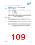
5.4.1.2
Start Field Definition
Table 5-6.
Start Field Bit Definitions
Bits[3:0] Encoding
Definition
0000
0010
0011
Start of cycle for a generic target
Grant for bus master 0
Grant for bus master 1
Stop/Abort: End of a cycle for a
target.
1111
NOTE: All other encodings are RESERVED.
108
Datasheet

 INTEL [ INTEL ]