DRAM Controller Registers (D0:F0)
5.1.6
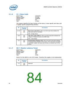
CC—Class Code
B/D/F/Type:
Address Offset:
Default Value:
Access:
0/0/0/PCI
09–0Bh
060000h
RO
Size:
24 bits
This register identifies the basic function of the device, a more specific sub-class, and
a register-specific programming interface.
Bit
Access &
Default
Description
23:16
RO
Base Class Code (BCC): This is an 8-bit value that indicates the
06h
base class code for the GMCH.
06h = Bridge device.
15:8
7:0
RO
00h
Sub-Class Code (SUBCC): This is an 8-bit value that indicates the
category of Bridge into which the GMCH falls.
00h = Host Bridge.
RO
00h
Programming Interface (PI): This is an 8-bit value that indicates
the programming interface of this device. This value does not specify
a particular register set layout and provides no practical use for this
device.
5.1.7
MLT—Master Latency Timer
B/D/F/Type:
Address Offset:
Default Value:
Access:
0/0/0/PCI
0Dh
00h
RO
Size:
8 bits
Device 0 in the GMCH is not a PCI master. Therefore this register is not implemented.
Bit
Access &
Default
Description
7:0
RO
Reserved
00h
84
Datasheet

 INTEL [ INTEL ]