DRAM Controller Registers (D0:F0)
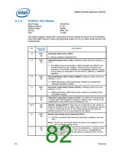
Bit
6
Access &
Default
Description
RO
0b
Reserved
5
RO
0b
66 MHz Capable: Does not apply to PCI Express. Hardwired to 0.
4
RO
1b
Capability List (CLIST): This bit is hardwired to 1 to indicate to the
configuration software that this device/function implements a list of
new capabilities. A list of new capabilities is accessed via register
CAPPTR at configuration address offset 34h. Register CAPPTR contains
an offset pointing to the start address within configuration space of
this device where the Capability Identification register resides.
3:0
RO
0h
Reserved
5.1.5
RID—Revision Identification
B/D/F/Type:
Address Offset:
Default Value:
Access:
0/0/0/PCI
8h
00h
RO
8 bits
Size:
This register contains the revision number of the GMCH Device 0. These bits are read
only and writes to this register have no effect.
Bit
Access &
Default
Description
7:0
RO
00h
Revision Identification Number (RID): This is an 8-bit value that
indicates the revision identification number for the GMCH Device 0.
Refer to the Intel® G35 Express Chipset Specification Update for the
value of the Revision ID register.
Datasheet
83

 INTEL [ INTEL ]