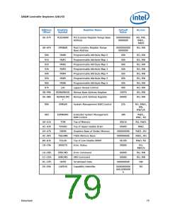
DRAM Controller Registers (D0:F0)
5.1.3
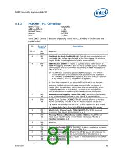
PCICMD—PCI Command
B/D/F/Type:
Address Offset:
Default Value:
Access:
0/0/0/PCI
4–5h
0006h
RO, RW
16 bits
Size:
Since GMCH Device 0 does not physically reside on PCI_A many of the bits are not
implemented.
Bit
Access &
Default
Description
15:10
9
RO
00h
Reserved
RO
0b
Fast Back-to-Back Enable (FB2B): This bit controls whether or not
the master can do fast back-to-back write. Since device 0 is strictly a
target, this bit is not implemented and is hardwired to 0.
8
RW
0b
SERR Enable (SERRE): This bit is a global enable bit for Device 0
SERR messaging. The GMCH does not have an SERR signal. The GMCH
communicates the SERR condition by sending an SERR message over
DMI to the ICH.
1= The GMCH is enabled to generate SERR messages over DMI for
specific Device 0 error conditions that are individually enabled in
the ERRCMD and DMIUEMSK registers. The error status is reported
in the ERRSTS, PCISTS, and DMIUEST registers.
0 =The SERR message is not generated by the GMCH for Device 0.
Note that this bit only controls SERR messaging for the Device 0.
Device 1 has its own SERRE bits to control error reporting for error
conditions occurring in that device. The control bits are used in a
logical OR manner to enable the SERR DMI message mechanism.
7
6
RO
0b
Address/Data Stepping Enable (ADSTEP): Address/data stepping
is not implemented in the GMCH, and this bit is hardwired to 0.
RW
0b
Parity Error Enable (PERRE): This bit controls whether or not the
Master Data Parity Error bit in the PCI Status register can bet set.
0= Master Data Parity Error bit in PCI Status register can NOT be set.
1 = Master Data Parity Error bit in PCI Status register CAN be set.
5
4
RO
0b
VGA Palette Snoop Enable (VGASNOOP): The GMCH does not
implement this bit and it is hardwired to a 0.
RO
0b
Memory Write and Invalidate Enable (MWIE): The GMCH will
never issue memory write and invalidate commands. This bit is
therefore hardwired to 0.
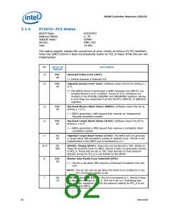
3
2
1
0
RO
0b
Reserved
RO
1b
Bus Master Enable (BME): The GMCH is always enabled as a master
on the backbone. This bit is hardwired to a 1.
RO
1b
Memory Access Enable (MAE): The GMCH always allows access to
main memory. This bit is not implemented and is hardwired to 1.
RO
0b
I/O Access Enable (IOAE): This bit is not implemented in the GMCH
and is hardwired to a 0.
Datasheet
81

 INTEL [ INTEL ]