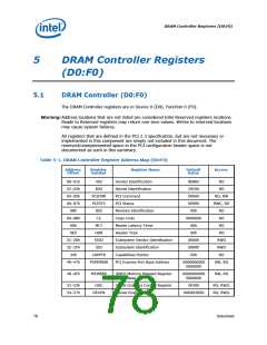
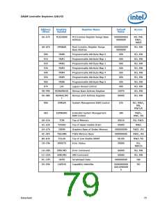
DRAM Controller Registers (D0:F0)
Address
Offset
Register
Symbol
Register Name
Default
Value
Access
60–67h
PCIEXBAR
PCI Express Register Range Base
Address
00000000E0
000000h
RO, RW,
RW/L,
RW/K
68–6Fh
DMIBAR
Root Complex Register Range
Base Address
0000000000
000000h
RO, RW
90h
91h
PAM0
PAM1
Programmable Attribute Map 0
Programmable Attribute Map 1
Programmable Attribute Map 2
Programmable Attribute Map 3
Programmable Attribute Map 4
Programmable Attribute Map 5
Programmable Attribute Map 6
Legacy Access Control
00h
00h
RO, RW
RO, RW
RO, RW
RO, RW
RO, RW
RO, RW
RO, RW
RO, RW
RO, RW
RO, RW
92h
PAM2
00h
93h
PAM3
00h
94h
PAM4
00h
95h
PAM5
00h
96h
PAM6
00h
97h
LAC
00h
98–99h
9A–9Bh
REMAPBASE
Remap Base Address Register
Remap Limit Address Register
03FFh
0000h
REMAPLIMI
T
9Dh
9Eh
SMRAM
System Management RAM Control
02h
38h
RO, RW/L,
RW,
RW/L/K
ESMRAMC
Extended System Management
RAM Control
RW/L,
RWC, RO
A0–A1h
A2–A3h
A4–A7h
AC–AFh
B0–B1h
C8–C9h
TOM
Top of Memory
0001h
0000h
RO, RW/L
RW/L
TOUUD
GBSM
Top of Upper Usable Dram
Graphics Base of Stolen Memory
TSEG Memory Base
00000000h
00000000h
0010h
RW/L ,RO
RW/L, RO
RW/L RO
TSEGMB
TOLUD
ERRSTS
Top of Low Usable DRAM
Error Status
0000h
RO,
RWC/S
CA–CBh
CC–CDh
DC–DFh
E0–E9h
ERRCMD
SMICMD
SKPD
Error Command
SMI Command
0000h
0000h
RO, RW
RO, RW
RW
Scratchpad Data
Capability Identifier
00000000h
CAPID0
0000000000
0001090009
h
RO
Datasheet
79

 INTEL [ INTEL ]