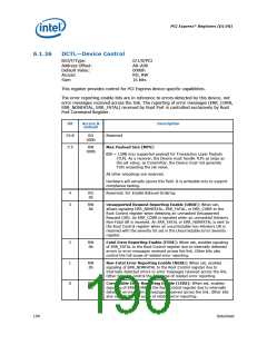
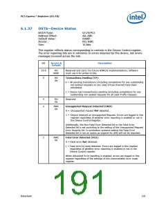
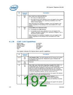
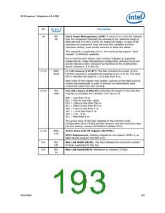
PCI Express* Registers (D1:F0)
6.1.39
LCTL—Link Control
B/D/F/Type:
Address Offset:
Default Value:
Access:
0/1/0/PCI
B0–B1h
0000h
RO, RW, RW/SC
16 bits
Size:
BIOS Optimal Default
0h
This register allows control of PCI Express link.
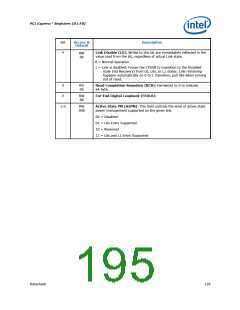
Bit
15:9
8
Access &
Default
Description
RO
0000000b
Reserved
Enable Clock Power Management (ECPM): Applicable only for form
factors that support a “Clock Request” (CLKREQ#) mechanism, this
enable functions as follows
RO
0b
0 = Disable. Clock power management is disabled and device must
hold CLKREQ# signal low (Default)
1 = Enable. Device is permitted to use CLKREQ# signal to power
manage link clock according to protocol defined in appropriate
form factor specification.
Components that do not support Clock Power Management (as
indicated by a 0b value in the Clock Power Management bit of the Link
Capabilities Register) must hardwire this bit to 0b.
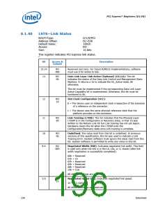
Extended Synch (ES):
7
RW
0b
0 = Standard Fast Training Sequence (FTS).
1 = Forces the transmission of additional ordered sets when exiting the
L0s state and when in the Recovery state.
This mode provides external devices (e.g., logic analyzers) monitoring
the Link time to achieve bit and symbol lock before the link enters L0
and resumes communication.
This is a test mode only and may cause other undesired side effects
such as buffer overflows or underruns.
Common Clock Configuration (CCC): The state of this bit affects
the L0s Exit Latency reported in LCAP[14:12] and the N_FTS value
advertised during link training. See PEGL0SLAT at offset 22Ch.
6
5
RW
0b
0 = This component and the component at the opposite end of this
Link are operating with asynchronous reference clock.
1 = This component and the component at the opposite end of this
Link are operating with a distributed common reference clock.
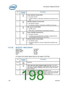
RW/SC
0b
Retrain Link (RL): This bit always returns 0 when read. This bit is
cleared automatically (no need to write a 0).
0 = Normal operation.
1 = Full Link retraining is initiated by directing the Physical Layer
LTSSM from L0, L0s, or L1 states to the Recovery state.
194
Datasheet

 INTEL [ INTEL ]