PCI Express* Registers (D1:F0)
Bit
Access &
Default
Description
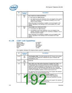
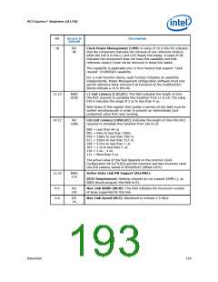
18
RO
0b
Clock Power Management (CPM): A value of 1b in this bit indicates
that the component tolerates the removal of any reference clock(s)
when the link is in the L1 and L2/3 Ready link states. A value of 0b
indicates the component does not have this capability and that
reference clock(s) must not be removed in these link states.
This capability is applicable only in form factors that support “clock
request” (CLKREQ#) capability.
For a multi-function device, each function indicates its capability
independently. Power Management configuration software must only
permit reference clock removal if all functions of the multifunction
device indicate a 1b in this bit.
17:15
14:12
RWO
010b
L1 Exit Latency (L1ELAT): This field indicates the length of time
this Port requires to complete the transition from L1 to L0. The value
010 b indicates the range of 2 us to less than 4 us.
Both bytes of this register that contain a portion of this field must be
written simultaneously in order to prevent an intermediate (and
undesired) value from ever existing.
RO
L0s Exit Latency (L0SELAT): Indicates the length of time this Port
100b
requires to complete the transition from L0s to L0.
000 = Less than 64 ns
001 = 64ns to less than 128ns
010 = 128ns to less than 256 ns
011 = 256ns to less than 512 ns
100 = 512ns to less than 1 us
101 = 1 us to less than 2 us
110 = 2 us – 4 us
111 = More than 4 us
The actual value of this field depends on the common Clock
Configuration bit (LCTL[6]) and the Common and Non-Common clock
L0s Exit Latency values in PEGL0SLAT (Offset 22Ch)
11:10
RWO
11b
Active State Link PM Support (ASLPMS):
BIOS Requirement: Desktop chipsets do not support ASPM L1, so
BIOS should program this field to 01.
9:4
3:0
RO
10h
Max Link Width (MLW): This field indicates the maximum number
of lanes supported for this link.
RO
1h
Max Link Speed (MLS): Hardwired to indicate 2.5 Gb/s.
Datasheet
193

 INTEL [ INTEL ]