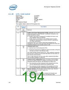
PCI Express* Registers (D1:F0)
Bit
Access &
Default
Description
4
Link Disable (LD): Writes to this bit are immediately reflected in the
value read from the bit, regardless of actual Link state.
RW
0b
0 = Normal operation
1 = Link is disabled. Forces the LTSSM to transition to the Disabled
state (via Recovery) from L0, L0s, or L1 states. Link retraining
happens automatically on 0 to 1 transition, just like when coming
out of reset.
3
2
RO
0b
Read Completion Boundary (RCB): Hardwired to 0 to indicate
64 byte.
RW
0b
Far-End Digital Loopback (FEDLB):
1:0
RW
Active State PM (ASPM): This field controls the level of active state
00b
power management supported on the given link.
00 = Disabled
01 = L0s Entry Supported
10 = Reserved
11 = L0s and L1 Entry Supported
Datasheet
195

 INTEL [ INTEL ]