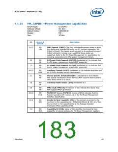
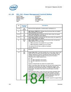
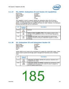
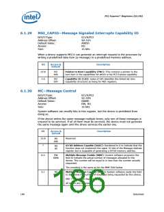
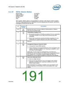
PCI Express* Registers (D1:F0)
Bit
Access &
Default
Description
0
RW
0b
MSI Enable (MSIEN): This bit controls the ability of this device to
generate MSIs.
0 = MSI will not be generated.
1 = MSI will be generated when we receive PME or HotPlug messages.
INTA will not be generated and INTA Status (PCISTS1[3]) will not
be set.
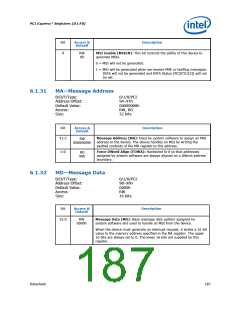
6.1.31
MA—Message Address
B/D/F/Type:
Address Offset:
Default Value:
Access:
0/1/0/PCI
94–97h
00000000h
RW, RO
Size:
32 bits
Bit
Access &
Default
Description
31:2
Message Address (MA): Used by system software to assign an MSI
address to the device. The device handles an MSI by writing the
padded contents of the MD register to this address.
RW
00000000h
1:0
Force DWord Align (FDWA): Hardwired to 0 so that addresses
assigned by system software are always aligned on a DWord address
boundary.
RO
00b
6.1.32
MD—Message Data
B/D/F/Type:
Address Offset:
Default Value:
Access:
0/1/0/PCI
98–99h
0000h
RW
Size:
16 bits
Bit
Access &
Default
Description
15:0
RW
Message Data (MD): Base message data pattern assigned by
0000h
system software and used to handle an MSI from the device.
When the device must generate an interrupt request, it writes a 32-bit
value to the memory address specified in the MA register. The upper
16 bits are always set to 0. The lower 16 bits are supplied by this
register.
Datasheet
187

 INTEL [ INTEL ]